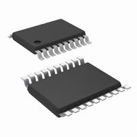
LM3100MH/NOPB National Semiconductor, LM3100MH/NOPB Datasheet - Page 4

LM3100MH/NOPB
Manufacturer Part Number
LM3100MH/NOPB
Description
IC REG SIMPLE SW 1.5A 20-TSSOP
Manufacturer
National Semiconductor
Series
PowerWise®, SIMPLE SWITCHER®r
Type
Step-Down (Buck)r
Datasheet
1.LM3100MHXNOPB.pdf
(18 pages)
Specifications of LM3100MH/NOPB
Internal Switch(s)
Yes
Synchronous Rectifier
Yes
Number Of Outputs
1
Voltage - Output
0.8 ~ 7 V
Current - Output
1.5A
Frequency - Switching
1MHz
Voltage - Input
4.5 ~ 36 V
Operating Temperature
-40°C ~ 125°C
Mounting Type
Surface Mount
Package / Case
20-TSSOP Exposed Pad, 20-eTSSOP, 20-HTSSOP
Dc To Dc Converter Type
Step Down
Pin Count
20
Input Voltage
36V
Output Voltage
0.8 to 7V
Switching Freq
1000KHz
Output Current
1.5A
Efficiency
86%
Package Type
TSSOP EP
Output Type
Adjustable
Switching Regulator
Yes
Mounting
Surface Mount
Input Voltage (min)
4.5V
Operating Temp Range
-40C to 125C
Operating Temperature Classification
Automotive
For Use With
LM3100EVAL - BOARD EVAL LM3100
Lead Free Status / RoHS Status
Lead free / RoHS Compliant
Power - Output
-
Lead Free Status / Rohs Status
Compliant
Other names
*LM3100MH
*LM3100MH/NOPB
LM3100MH
*LM3100MH/NOPB
LM3100MH
www.national.com
Start-Up Regulator, V
Switching Characteristics
Soft-start
Current Limit
ON/OFF Timer
Enable Input
Regulation and Over-Voltage Comparator
VIN, RON to GND
SW to GND
SW to GND (Transient)
VIN to SW
BST to SW
All Other Inputs to GND
Absolute Maximum Ratings
If Military/Aerospace specified devices are required,
please contact the National Semiconductor Sales Office/
Distributors for availability and specifications.
Electrical Characteristics
over the full Operating Junction Temperature (T
statistical correlation. Typical values represent the most likely parametric norm at T
purposes only. Unless otherwise stated the following conditions apply: V
V
t
R
CC-UVLO-HYS
R
VCC-UVLO-D
V
V
Symbol
V
V
DS- DN-ON
t
DS-UP-ON
V
IN
CC-UVLO
ON-MIN
I
I
G-UVLO
EN-HYS
V
IN-SD
t
V
VCCL
V
FB-OV
I
t
I
OFF
I
I
ON
- V
SS
CL
FB
IN
CC
EN
FB
CC
V
V
V
V
(UVLO)
V
V
I
I
Main MOSFET Rds(on)
Syn. MOSFET Rds(on)
Gate drive voltage UVLO
SS pin source current
Syn. MOSFET current limit threshold
ON timer pulse width
ON timer minimum pulse width
OFF timer pulse width
EN Pin input threshold
Enable threshold hysteresis
In-regulation feedback voltage
Feedback over-voltage threshold
IN
IN
CC
IN
CC
CC
CC
CC
CC
operating current
operating current, Device shutdown V
- V
output voltage
current limit (Note 4)
under-voltage lockout threshold
UVLO hysteresis
UVLO filter delay
CC
dropout voltage
Parameter
Specifications with standard type are for T
-2V (< 100ns)
(Note
J
-0.3V to 40V
-0.3V to 40V
-0.3V to 40V
) range. Minimum and Maximum limits are guaranteed through test, design, or
-0.3V to 7V
-0.3V to 7V
1)
C
I
I
V
V
V
No switching, V
V
V
V
V
V
V
V
V
T
T
CC
CC
J
J
CC
IN
IN
EN
BST
SS
IN
IN
EN
EN
SS
SS
CC
= −40°C to + 125°C
= 0°C to + 125°C
= 2mA
= 20mA
increasing
decreasing
= 10V, R
= 30V, R
= 0.5V
≥
≥
4
= 0V
= 0V
rising
falling
= 680nF, no load
- V
0.8V
0.8V
Conditions
SW
ESD Rating
Storage Temperature Range
Junction Temperature (T
Supply Voltage Range (VIN)
Junction Temperature Range (T
Thermal Resistance (θ
Operating Ratings
Human Body Model
increasing
ON
ON
IN
= 18V, V
FB
= 100 kΩ
= 100 kΩ
= 1V
(Note
J
OUT
= 25°C, and are provided for reference
2)
J
= 3.3V.
= 25°C only; limits in boldface type apply
1.236
0.784
0.788
0.894
JC
Min
5.0
3.6
40
6
)
J
)
(Note
J
3)
)
(Note
0.920
3.75
0.18
0.11
1.38
0.47
1.26
Typ
350
130
200
260
6.0
0.7
3.3
1.9
0.8
50
65
17
90
3
8
5
1)
−40°C to + 125°C
-65°C to +150°C
1.285
0.816
0.812
0.940
Max
3.85
0.35
140
570
100
7.2
0.2
9.8
30
1
4
4.5V to 36V
6.5°C/W
150°C
Units
±2kV
mV
mA
mV
mA
mV
µA
µA
nA
µs
µs
ns
ns
Ω
Ω
V
V
V
A
V
V
V


