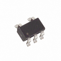
MAX829EUK+T Maxim Integrated Products, MAX829EUK+T Datasheet - Page 7

MAX829EUK+T
Manufacturer Part Number
MAX829EUK+T
Description
IC INVERTER VOLT SOT23-5
Manufacturer
Maxim Integrated Products
Type
Switched Capacitor (Charge Pump), Doubler, Invertingr
Datasheet
1.MAX828EUKT.pdf
(8 pages)
Specifications of MAX829EUK+T
Internal Switch(s)
Yes
Synchronous Rectifier
No
Number Of Outputs
1
Voltage - Output
-1.15 ~ 6 V, ±2.3 ~ ±12 V
Current - Output
25mA
Frequency - Switching
35kHz
Voltage - Input
1.5 ~ 5.5 V
Operating Temperature
-40°C ~ 85°C
Mounting Type
Surface Mount
Package / Case
SOT-23-5, SC-74A, SOT-25
Function
Inverting
Output Voltage
- 1.5 V to - 5.5 V
Output Current
25 mA
Supply Current
150 uA
Maximum Operating Temperature
+ 85 C
Input Voltage
1.5 V to 5.5 V
Maximum Power Dissipation
571 mW
Minimum Operating Temperature
- 40 C
Mounting Style
SMD/SMT
Switching Frequency
35 KHz
Lead Free Status / RoHS Status
Lead free / RoHS Compliant
Power - Output
-
Lead Free Status / Rohs Status
Lead free / RoHS Compliant
When under heavy loads, where higher supply is sourcing
current into OUT, the OUT supply must not be pulled
above ground. Applications that sink heavy current into
OUT require a Schottky diode (1N5817) between GND
and OUT, with the anode connected to OUT (Figure 7).
Good layout is important, primarily for good noise perfor-
mance. To ensure good layout, mount all components as
close together as possible, keep traces short to mini-
mize parasitic inductance and capacitance, and use a
ground plane.
Figure 4. Cascading MAX828s or MAX829s to Increase
Output Voltage
Figure 6. Combined Doubler and Inverter
C1
C1
3
4
5
3
4
5
MAX828
MAX829
MAX828
MAX829
“1”
_______________________________________________________________________________________
Heavy Output Current Loads
C3
2
1
Switched-Capacitor Voltage Inverters
C1
2
1
+V
+V
Layout and Grounding
IN
IN
…
…
C2
D2
D1
3
4
5
V
OUT
MAX828
MAX829
D1, D2 = 1N4148
C2
C4
“n”
= -nV
V
(V
V
OUT
OUT
FD1
IN
= (2V
) - (V
= -V
2
1
IN
FD2
IN
) -
)
V
C2
OUT
For a similar device with logic-controlled shutdown,
please refer to the MAX1719/MAX1720/MAX1721. To
add manual shutdown control to the MAX828/MAX829,
use the circuit in Figure 8. The output resistance of the
MAX828/MAX829 will typically be 20Ω plus two times
the output resistance of the buffer driving IN. The 0.1µF
capacitor at the IN pin absorbs the transient input cur-
rents of the MAX828/MAX829.
The output resistance of the buffer driving the IN pin can
be reduced by connecting multiple buffers in parallel.
The polarity of the SHUTDOWN signal can also be
changed by using a noninverting buffer to drive IN.
Figure 5. Paralleling MAX828s or MAX829s to Reduce Output
Resistance
Figure 7. High V- Load Current
C1
Shutting Down the MAX828/MAX829
3
4
5
MAX828
MAX829
“1”
MAX828
MAX829
2
1
C1
+V
IN
R
GND
OUT
OUT
=
…
…
4
1
R
NUMBER OF DEVICES
5
3
4
OUT
OF SINGLE DEVICE
V
OUT
MAX828
MAX829
“n”
= -V
IN
2
1
V
C2
OUT
7


