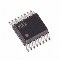
MAX686EEE+T Maxim Integrated Products, MAX686EEE+T Datasheet - Page 11

MAX686EEE+T
Manufacturer Part Number
MAX686EEE+T
Description
IC SUPPLY LCD BIAS INV 16-QSOP
Manufacturer
Maxim Integrated Products
Type
Step-Up (Boost), Invertingr
Datasheet
1.MAX686EEE.pdf
(16 pages)
Specifications of MAX686EEE+T
Internal Switch(s)
Yes
Synchronous Rectifier
No
Number Of Outputs
1
Voltage - Output
±27.5V
Current - Output
100mA
Frequency - Switching
300kHz
Voltage - Input
2.7 ~ 5.5 V
Operating Temperature
-40°C ~ 85°C
Mounting Type
Surface Mount
Package / Case
16-QSOP
Power - Output
667mW
Lead Free Status / RoHS Status
Lead free / RoHS Compliant
Note that for a positive output voltage, V
as V
V
V
For a negative output voltage, the FB threshold voltage
(V
(Figures 2 and 3). Again, choose R1 to be 120k
that the current in the divider is about 10µA. Then
determine R2 as follows:
For example, if V
Assume V
then determine R3 and V
For a negative output voltage,
At power-up, the DAC resets to mid-scale where V
= 0.635V. Therefore, the output voltage after reset is:
Note that for a negative output voltage,
es as V
V
V
The MAX686 may be used without the DAC to control
the output voltage. For either positive or negative out-
put voltage applications, set the MAX686’s output volt-
age using only two external resistors (R1 and R2) as
shown in Figure 1, 2, or 3. Since the input bias current
at FB has a 50nA maximum value, large resistors can
be used in the feedback loop without a significant loss
of accuracy. Select R1 to be in the 10k
range and calculate R2 using the applicable equations
from the following subsections.
Use the circuit of Figure 1, connecting POL to GND and
omitting R3. Connecting POL to GND sets the threshold
voltage at FB to V
10k to 220k range and calculate R2 as follows:
where V
DACOUT
DACOUT
DACOUT
DACOUT
FB
V
R3 = R2 x (V
) is 0V, and R1 is placed between FB and REF
DACOUT
OUT
Setting the Maximum Negative Output Voltage
Setting the Minimum Negative Output Voltage
V
= 1.2M x (0 - 1.25) / (-25 - -12.5) =120kΩ
DACOUT
REF
R2 = 120k x
OUT(MID)
V
= V
= 1.25V.
= 0V.
OUT(MAX)
= 1.25V, and
OUT(MIN)
= 0V, and V
= 1.25V.
OUT(MIN)
decreases. V
R2 = R1 x
R2 = R1 x
increases.
OUT(MIN)
FB
= -12.5 + (0 - 0.635) x (1.2M) /
Setting the Positive Output Voltage
______________________________________________________________________________________
REF
- V
)
(120k) = -18.85V
Setting the Output Voltage
= -25V and V
DACOUT(MAX)
|
. Choose the value of R1 in the
+ (V
(-12.5) / (1.25)
OUT(MID)
(
LCD Bias Supply with Internal Switch
V
|
= -12.5V:
|
OUT(MIN)
V
V
FB
OUT
|
OUT
V
OUT(MIN)
OUT(MAX)
OUT(MAX)
- V
/ V
/ V
DACOUT
as follows:
REF
without the DAC
REF
OUT(MIN)
) / (V
|
|
corresponds to
= 1.2M
-1
|
corresponds to
corresponds to
|
|
corresponds to
)
OUT(MAX)
) x R2 / R3.
V
OUT
OUT
DAC-Controlled Boost/Inverter
increases
= -12.5V,
to 220k
|
DACOUT
increas-
-
so
For negative output voltages, configure R1 and R2 as
shown in Figures 2 and 3, connecting POL to V
omitting R3. Connecting POL to V
old voltage to GND for negative output voltages.
Choose R1 in the 10k
R2 as follows:
where V
Figures 2 and 3 demonstrate two possible methods of
generating a negative voltage with the MAX686. In
Figure 3, D2 connects to the input supply (V
connection features the best output ripple perfor-
mance, but
-27.5V - V
tive voltage, use the method of Figure 2, connecting D2
to GND. This method allows a maximum output voltage
of -27.5V, but
External current-limit selection provides added control
over the MAX686’s output performance. A higher cur-
rent limit increases the amount of energy stored in the
inductor during each cycle, which provides higher out-
put current capability. For higher output current appli-
cations, choose the 500mA current-limit option by
connecting ISET to V
output current, the 250mA current limit provides several
advantages. First, a smaller inductor saves board area
and cost. Second, smaller energy transfers per cycle
reduce output ripple for a given capacitor. Connecting
ISET to GND selects the 250mA current-limit option.
Connecting ISET to V
option. Refer to the Typical Operating Characteristics
for efficiency and load current graphs at each ISET cur-
rent setting.
The MAX686’s high switching frequency allows for the
use of a small inductor. The 22µH inductor shown in
Figures 1, 2, and 3 is recommended for most applica-
tions, although values between 10µH and 47µH are
acceptable. Use inductors with a ferrite core or equiva-
lent; powder iron cores are not recommended for use
with high switching frequencies. The inductor’s incre-
mental saturation rating must exceed the selected cur-
rent limit. For highest efficiency, use an inductor with a
low DC resistance (under 200m ). See Table 1 for a list
of inductor suppliers.
Setting the Peak Inductor Current Limit
REF
IN
= 1.25V.
. If the application requires a larger nega-
|
V
|
OUT
V
OUT
R2 = R1 x
Setting the Negative Output Voltage
|
must be limited to values less than
|
must be greater than V
CC
CC
. When the load requires lower
selects the 500mA current-limit
to 220k
|
V
OUT
Selecting Inductors
|
/ V
CC
range and calculate
REF
sets the FB thresh-
IN
.
IN
CC
). This
and
11


