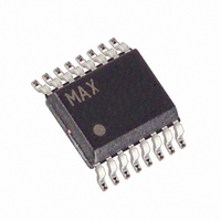
MAX686EEE+T Maxim Integrated Products, MAX686EEE+T Datasheet - Page 9

MAX686EEE+T
Manufacturer Part Number
MAX686EEE+T
Description
IC SUPPLY LCD BIAS INV 16-QSOP
Manufacturer
Maxim Integrated Products
Type
Step-Up (Boost), Invertingr
Datasheet
1.MAX686EEE.pdf
(16 pages)
Specifications of MAX686EEE+T
Internal Switch(s)
Yes
Synchronous Rectifier
No
Number Of Outputs
1
Voltage - Output
±27.5V
Current - Output
100mA
Frequency - Switching
300kHz
Voltage - Input
2.7 ~ 5.5 V
Operating Temperature
-40°C ~ 85°C
Mounting Type
Surface Mount
Package / Case
16-QSOP
Power - Output
667mW
Lead Free Status / RoHS Status
Lead free / RoHS Compliant
The MAX686 is a step-up converter that contains an
internal N-channel MOSFET switch to convert a +0.8V
to +27.5V battery voltage to a higher positive or a nega-
tive voltage. Figure 1 shows the MAX686 configured to
produce a positive output voltage. Figure 2 shows the
MAX686 configured with one additional diode and
capacitor to produce a negative output voltage. Figure
3 shows an alternative method for developing negative
output voltages. Set the output voltage with an external
resistor-divider network. Adjust the output voltage with
the internal digital-to-analog converter (DAC). The
MAX686’s current-limited pulse-frequency-modulation
(PFM) control scheme has programmable current limit-
ing and provides high efficiency over a wide range of
load conditions.
A combination of peak current limiting and a pair of one-
shots controls the MAX686 switching. During the on-
cycle, the internal switch closes, and current through
the inductor ramps up until either the fixed 10µs maxi-
mum on-time expires (at low input voltages) or the
switch peak current limit is reached. The peak current
limit is selectable to either 500mA (ISET = V
250mA (ISET = GND) (see the section Setting the Peak
Inductor Current Limit ).
Figure 3. Alternative Negative Output Voltage Application Circuit
Boost Control Scheme (POL = GND)
V
IN
= 0.8V TO 27.5V
V
_______________________________________________________________________________________
CC
= 2.7V TO 5.5V
Detailed Description
LCD Bias Supply with Internal Switch
DAC CONTROL
15 F
0.1 F
ON/OFF
DAC-Controlled Boost/Inverter
V
V
POL
UP
DN
SHDN
CC
DD
GND
CC
MAX686
22 H
L1
) or
DACOUT
LCDON
PGND
ISET
POK
REF
LX
FB
After the on-cycle terminates, the switch turns off, and
the inductor charges the output capacitor through the
diode. If the output is out of regulation after the mini-
mum off-time has transpired, another on-cycle begins.
If the output is within regulation when the minimum off-
time transpires, the off-cycle extends until the output
falls out of regulation, at which point an on-cycle starts.
The MAX686 regulates the voltage on FB (V
1.25V. When the output is well below regulation (V
less than 1V and the switch current limit is exceeded),
the MAX686 operates in initial power-up mode, and the
minimum off-time increases to 5µs to provide soft-start.
The switching frequency, which depends on the load,
the input voltage, and the output voltage, can be as
high as 300kHz.
In inverting operation, the MAX686 regulates the volt-
age on FB (V
is reversed. The minimum off-time changes to 3.5µs for
negative output voltages. When the output is well below
regulation (V
limit is exceeded), initial power-up is assumed, and the
minimum off-time increases to 5µs to provide soft-start.
D2
MBR0530L
Inverting Control Scheme (POL = V
R3
2
R4
R1
0.1 F
FB
FB
2.2 F
) to 0V, and the error amplifier’s polarity
is 0.25V or more and the switch current
R2
C
470pF
F
|
V
2.2 F
OUT
|
NEGATIVE
VOLTAGE
OUTPUT
D1
MBR0530L
(27.5V - V
IN
)
FB
FB
CC
) to
is
9
)


