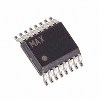
MAX1637EEE Maxim Integrated Products, MAX1637EEE Datasheet - Page 17

MAX1637EEE
Manufacturer Part Number
MAX1637EEE
Description
IC CTRLR MINI LV STPDWN 16-QSOP
Manufacturer
Maxim Integrated Products
Type
Step-Down (Buck)r
Datasheet
1.MAX1637EEE.pdf
(20 pages)
Specifications of MAX1637EEE
Internal Switch(s)
No
Synchronous Rectifier
Yes
Number Of Outputs
1
Voltage - Output
1.1 ~ 5.5 V
Current - Output
3A
Frequency - Switching
Adj to 350kHz
Voltage - Input
3.15 ~ 5.5 V
Operating Temperature
-40°C ~ 85°C
Mounting Type
Surface Mount
Package / Case
16-QSOP
Power - Output
667mW
Lead Free Status / RoHS Status
Contains lead / RoHS non-compliant
Available stocks
Company
Part Number
Manufacturer
Quantity
Price
Company:
Part Number:
MAX1637EEE
Manufacturer:
MAXIM
Quantity:
77
Part Number:
MAX1637EEE
Manufacturer:
MAXIM/美信
Quantity:
20 000
Company:
Part Number:
MAX1637EEE+
Manufacturer:
MAXIM
Quantity:
651
Company:
Part Number:
MAX1637EEE+T
Manufacturer:
MAXIM
Quantity:
44 000
Part Number:
MAX1637EEE+T
Manufacturer:
MAXIM/美信
Quantity:
20 000
The rectifier is a clamp across the low-side MOSFET
that catches the negative inductor swing during the
60ns dead time between turning one MOSFET off and
turning each low-side MOSFET on. The latest genera-
tions of MOSFETs incorporate a high-speed silicon
body diode, which serves as an adequate clamp diode
if efficiency is not of primary importance. A Schottky
diode can be placed in parallel with the body diode to
reduce the forward voltage drop, typically improving
efficiency 1% to 2%. Use a diode with a DC current rat-
ing equal to one-third of the load current; for example,
use an MBR0530 (500mA-rated) type for loads up to
1.5A, a 1N5819 type for loads up to 3A, or a 1N5822
type for loads up to 10A. The rectifier’s rated reverse-
breakdown voltage must be at least equal to the maxi-
mum input voltage, preferably with a 20% margin.
A signal diode such as a 1N4148 works well in most
applications. Do not use large power diodes, such as
1N5817 or 1N4001.
Low input voltages and low input-output differential volt-
ages each require extra care in their design. Low
V
sag when the load current changes abruptly. The sag’s
amplitude is a function of inductor value and maximum
duty factor (D
ter, 93% guaranteed over temperature at f = 200kHz) as
follows:
Table 5 is a low-voltage troubleshooting guide. The
cure for low-voltage sag is to increase the output
capacitor’s value. For example, at V
5V, L = 10µH, ƒ = 200kHz, and I
capacitance of 660µF keeps the sag below 200mV.
Note that only the capacitance requirement increases;
the ESR requirements do not change. Therefore, the
Table 5. Low-Voltage Troubleshooting Guide
IN
Sag or droop in V
under step-load change
Dropout voltage is
too high
V
-V
SAG
OUT
SYMPTOM
= [(I
differentials can cause the output voltage to
V
OUT
STEP
MAX
)]
OUT
, an Electrical Characteristics parame-
)
______________________________________________________________________________________
2
x L] / [2C
Low-Voltage Operation
Low V
under 1.5V
Low V
under 1V
F
Boost-Supply Diode D2
Rectifier Clamp Diode
x (V
IN
IN
CONDITION
-V
-V
IN(MIN)
STEP
OUT
OUT
IN
= 5.5V, V
Precision Step-Down Controller
differential,
differential,
= 3A, a total
x D
MAX
OUT
-
=
Limited inductor-current
slew rate per cycle
Maximum duty-cycle limits
exceeded
Miniature, Low-Voltage,
added capacitance can be supplied by a low-cost bulk
capacitor in parallel with the normal low-ESR capacitor.
The major efficiency-loss mechanisms under loads are
as follows, in the usual order of importance:
• P(I
• P(tran) = transition losses
• P(gate) = gate-charge losses
• P(diode) = diode-conduction losses
• P(cap) = capacitor ESR losses
• P(IC) = losses due to the IC’s operating supply current
Inductor core losses are fairly low at heavy loads
because the inductor’s AC current component is small.
Therefore, these losses are not considered in this
analysis. Ferrite cores are preferred, especially at
300kHz, but powdered cores, such as Kool-Mu, can
also work well.
where R
the MOSFET on-resistance, and R
sense resistor value. The R
tical MOSFETs for the high-side and low-side switches
because they time-share the inductor current. If the
MOSFETs are not identical, their losses can be estimat-
ed by averaging the losses according to duty factor.
where C
high-side MOSFET (a data sheet parameter), I
the DH gate-driver peak output current (1.5A typ), and
the rise/fall time of the DH driver is typically 20ns.
ROOT CAUSE
__________Applications Information
Efficiency = P
P
P = (I
PD(tran) = transition loss = V
[(V
TOTAL
2
R) = I
Heavy-Load Efficiency Considerations
IN
DC
RSS
2
C
R) = I
RSS
2
= P(I
is the DC resistance of the coil, R
R losses
is the reverse transfer capacitance of the
= P
P(cap) + P(IC)
LOAD
/ I
2
OUT
OUT
GATE
R) + P(tran) + P(gate) + P(diode) +
2
/ P
/ (P
x (R
) + 20ns]
Increase bulk output capacitance
per formula (see Low-Voltage
Operation section). Reduce
inductor value.
Reduce operation to 200kHz.
Reduce MOSFET on-resistance
and coil DC resistance.
IN
OUT
DC
x 100%
DS(ON)
+ R
+ P
TOTAL
DS(ON)
SOLUTION
SENSE
term assumes iden-
IN
) x 100%
x I
+R
is the current-
LOAD
SENSE
DS(ON)
GATE
)
x ƒ x
17
is
is


