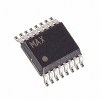
MAX1637EEE Maxim Integrated Products, MAX1637EEE Datasheet - Page 18

MAX1637EEE
Manufacturer Part Number
MAX1637EEE
Description
IC CTRLR MINI LV STPDWN 16-QSOP
Manufacturer
Maxim Integrated Products
Type
Step-Down (Buck)r
Datasheet
1.MAX1637EEE.pdf
(20 pages)
Specifications of MAX1637EEE
Internal Switch(s)
No
Synchronous Rectifier
Yes
Number Of Outputs
1
Voltage - Output
1.1 ~ 5.5 V
Current - Output
3A
Frequency - Switching
Adj to 350kHz
Voltage - Input
3.15 ~ 5.5 V
Operating Temperature
-40°C ~ 85°C
Mounting Type
Surface Mount
Package / Case
16-QSOP
Power - Output
667mW
Lead Free Status / RoHS Status
Contains lead / RoHS non-compliant
Available stocks
Company
Part Number
Manufacturer
Quantity
Price
Company:
Part Number:
MAX1637EEE
Manufacturer:
MAXIM
Quantity:
77
Part Number:
MAX1637EEE
Manufacturer:
MAXIM/美信
Quantity:
20 000
Company:
Part Number:
MAX1637EEE+
Manufacturer:
MAXIM
Quantity:
651
Company:
Part Number:
MAX1637EEE+T
Manufacturer:
MAXIM
Quantity:
44 000
Part Number:
MAX1637EEE+T
Manufacturer:
MAXIM/美信
Quantity:
20 000
Miniature, Low-Voltage,
Precision Step-Down Controller
where Q
side and high-side switches. For matched MOSFETs,
Q
MOSFET. Efficiency can usually be optimized by con-
necting V
the system +5V supply.
where t
V
pated in the MOSFET body diode if no external
Schottky diode is used.
where I
the Input Capacitor Value section.
Under light loads, the PWM operates in discontinuous
mode. The inductor current discharges to zero at some
point during the charging cycle. This makes the induc-
tor current’s AC component high compared to the load
current, which increases core losses and I
the input-output filter capacitors. For best light-load effi-
ciency, use MOSFETs with moderate gate-charge lev-
els and use ferrite MPP or other low-loss core material.
Avoid powdered-iron cores; even Kool-Mu (aluminum
alloy) is not as desirable as ferrite.
Noise-sensitive applications such as hi-fidelity multi-
media-equipped systems, cellular phones, RF commu-
nicating computers, and electromagnetic pen-entry
systems should operate the controller in PWM mode
(SKIP = high). This mode forces a constant switching
frequency, reducing interference due to switching
noise by concentrating the radiated EM fields at a
known frequency outside the system audio or IF bands.
Choose an oscillator frequency for which switching-
frequency harmonics do not overlap a sensitive fre-
quency band. If necessary, synchronize the oscillator
to a tight-tolerance external clock generator.
The circuit of Figure 7 is powered from a single 3.3V to
5.5V source and delivers 4A at 2.5V. At input voltages
of 3.15V, this circuit typically achieves efficiencies of
90% at 3.5A load currents. When using a single supply
to power both V
exceed the 5.5V rating (6V absolute maximum) for V
18
FWD
g
P(cap) = input capacitor ESR loss = I
P(diode) = diode conduction losses = I
is twice the data-sheet value of an individual
______________________________________________________________________________________
is the diode forward voltage. This power is dissi-
D
RMS
Light-Load Efficiency Considerations
g
is the diode conduction time (120ns typ), and
GG
P(gate) = Q
is the sum of the gate-charge values for low-
is the input ripple current as calculated in
to the most efficient 5V source, such as
x t
BATT
D
x ƒ
and V
g
x ƒ x V
Powering From a Single
BIAS
Low-Noise Operation
Low-Voltage Supply
GG
, be sure that it does not
RMS
LOAD
2
2
R losses in
x R
x V
ESR
FWD
GG
and V
may cause transient dips on V
decoupling capacitor on V
increased to 2µF or greater. This circuit uses low-
threshold (specified at V
which allow a typical startup of 3.15V at above 4A. Low
input voltages demand the use of larger input capaci-
tors. Sanyo OS-CONs are recommended for their high
capacity and low ESR.
Good PC board layout is required to achieve specified
noise, efficiency, and stable performance. The PC
board layout artist must be given explicit instructions,
preferably a pencil sketch showing the placement of
power-switching components and high-current routing.
See the PC board layout in the MAX1637 evaluation kit
manual for examples. A ground plane is essential for
optimum performance. In most applications, the circuit
will be located on a multi-layer board, and full use of
the four or more copper layers is recommended. Use
the top layer for high-current connections, the bottom
layer for quiet connections (REF, CC, GND), and the
inner layers for an uninterrupted ground plane. Use the
following step-by-step guide:
1) Place the high-power components (C1, C2, Q1, Q2,
Ideally, surface-mount power components are butted
up to one another with their ground terminals almost
touching. These high-current grounds are then con-
nected to each other with a wide, filled zone of
top-layer copper so they do not go through vias. The
resulting top-layer subground plane is connected to the
normal inner-layer ground plane at the output ground
terminals, which ensures that the IC’s analog ground is
D1, L1, and R1) first, with their grounds adjacent.
• Minimize current-sense resistor trace lengths and
• Minimize ground trace lengths in the high-current
• Minimize other trace lengths in the high-current
ensure accurate current sensing with Kelvin con-
nections (Figure 8).
paths.
paths.
— Use >5mm-wide traces.
— CIN to high-side MOSFET drain: 10mm
— Rectifier diode cathode to low side
— MOSFET: 5mm max length
— LX node (MOSFETs, rectifier cathode, induc-
CC
max length
tor): 15mm max length
. Also, heavy current surges from the input
PC Board Layout Considerations
GS
= 2.7V) IRF7401 MOSFETs
CC
CC
. To prevent this, the
may need to be


