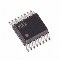
MAX1677EEE Maxim Integrated Products, MAX1677EEE Datasheet - Page 8

MAX1677EEE
Manufacturer Part Number
MAX1677EEE
Description
IC CONV DC-DC STEP-UP 16-QSOP
Manufacturer
Maxim Integrated Products
Type
Step-Up (Boost)r
Datasheet
1.MAX1677EEE.pdf
(16 pages)
Specifications of MAX1677EEE
Internal Switch(s)
Yes
Synchronous Rectifier
Yes
Number Of Outputs
2
Voltage - Output
3.3V or Adj Main, -28 ~ 28 V or Adj Secondary
Current - Output
350mA
Frequency - Switching
300kHz
Voltage - Input
0.7 ~ 5.5 V
Operating Temperature
-40°C ~ 85°C
Mounting Type
Surface Mount
Package / Case
16-QSOP
Power - Output
696mW
Output Voltage
2.5 V to 5.5 V
Output Current
350 mA
Input Voltage
0.7 V to 5.5 V
Supply Current
35 uA
Switching Frequency
300 KHz
Mounting Style
SMD/SMT
Maximum Operating Temperature
+ 85 C
Minimum Operating Temperature
- 40 C
Lead Free Status / RoHS Status
Contains lead / RoHS non-compliant
Available stocks
Company
Part Number
Manufacturer
Quantity
Price
Company:
Part Number:
MAX1677EEE
Manufacturer:
MAXIM
Quantity:
247
Part Number:
MAX1677EEE
Manufacturer:
MAXIM/美信
Quantity:
20 000
Part Number:
MAX1677EEE+
Manufacturer:
MAXIM/美信
Quantity:
20 000
Compact, High-Efficiency, Dual-Output
Step-Up and LCD Bias DC-DC Converter
Dual Mode is a trademark of Maxim Integrated Products.
The MAX1677 is a highly-efficient, dual-output power
supply for battery-powered devices. On-chip are two
complete step-up DC-DC converters to power main
logic and bias an LCD (Figure 1). The main boost con-
verter (MBC) has on-chip P-channel and N-channel
MOSFETs that provide synchronous-rectified voltage
conversion for maximum efficiency at loads up to
300mA. See Table 1 for available output current with
typical battery configurations. The output voltage of the
MBC is factory-preset to 3.3V, or can be set from 2.5V
to 5.5V with external resistors (dual-mode operation).
Either fixed-frequency PWM or low-operating-current
PFM operation can be selected for the MBC using the
CLK/SEL input (Table 2).
8
PIN
10
11
12
13
14
15
16
_______________________________________________________________________________________
1
2
3
4
5
6
7
8
9
LCDGND
CLK/SEL
LCDPOL
LCDON
LCDFB
LCDLX
NAME
PGND
POUT
GND
OUT
LBO
REF
LBI
ON
FB
LX
Output Sense Input. The device is powered from OUT. Bypass to GND with a 0.1µF ceramic capacitor.
Connect OUT to POUT through a 10Ω series resistor.
Dual Mode™ Main Boost Feedback Input. Connect to GND for 3.3V output. Connect a voltage-divider from
OUT to FB to adjust the output in the 2.5V to 5.5V range (Figure 5).
Low-Battery-Comparator Input. Threshold is 614mV. Set the low-battery trip-point with an external voltage
divider (Figure 7).
Open-Drain, Low-Battery Output. LBO is low when LBI is below 614mV, otherwise it remains high.
Sync Clock and PWM Select Input.
CLK/SEL = low: low-power, low-quiescent-current PFM mode.
CLK/SEL = high: low-noise, high-power PWM mode at 300kHz.
CLK/SEL = driven with external clock of 200kHz to 400kHz, synchronized PWM high-power mode.
LCD Enable Input. Drive high to turn on LCD boost converter. Main DC-DC must also be on.
LCD Polarity Select Input. Sets LCD boost converter polarity and peak current output (Table 2).
1.25V Reference Output. Bypass with 0.1µF.
Ground
LCD Feedback Input. Threshold is 1.25V for positive with LCDPOL high, and 0 for negative with
LCDPOL low.
I.C. Enable Input. Drive high to enable the MAX1677.
LCD Boost 28V Switch Drain
Source of the Internal N-Channel DMOS LCD Boost-Converter Switch
Source of the Internal N-Channel Main Boost-Converter Switch
Main Output Boost Internal Switch Drain
Boost DC-DC Converter Power Output. Source of internal P-channel MOSFET main boost-converter
synchronous rectifier.
Detailed Description
The LCD boost converter (LCD) includes an internal N-
channel DMOS switch to generate positive or negative
voltages up to ±28V. The polarity of the LCD output is
set by LCDPOL input (Table 3). Figure 2 shows the
MAX1677 configured for a positive LCD output voltage
with a 3.3V main output. Figure 3 shows the MAX1677
configured for a negative LCD output. LCDPOL also
allows the current limit of LCDLX to be reduced from
350mA to 225mA to allow minimum-size inductors in
low-current LCD applications (typically for LCD loads
<10mA).
Also included in the MAX1677 are a precision 1.25V
reference that sources up to 50µA, logic shutdown con-
trol for the MBC and LCD (the MBC must be on for the
LCD to operate), and a low-battery comparator.
FUNCTION
Pin Description


