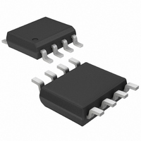
MAX1951ESA+ Maxim Integrated Products, MAX1951ESA+ Datasheet - Page 10

MAX1951ESA+
Manufacturer Part Number
MAX1951ESA+
Description
IC DC-DC PWM SW REG 2A 8-SOIC
Manufacturer
Maxim Integrated Products
Type
Step-Down (Buck)r
Datasheet
1.MAX1952ESA.pdf
(15 pages)
Specifications of MAX1951ESA+
Internal Switch(s)
Yes
Synchronous Rectifier
Yes
Number Of Outputs
1
Voltage - Output
0.8 ~ 5.5 V
Current - Output
2A
Frequency - Switching
1MHz
Voltage - Input
2.6 ~ 5.5 V
Operating Temperature
-40°C ~ 85°C
Mounting Type
Surface Mount
Package / Case
8-SOIC (3.9mm Width)
Power - Output
976mW
Output Voltage
0.8 V
Output Current
2 A
Input Voltage
2.6 V to 5.5 V
Supply Current
6 mA
Switching Frequency
1 MHz
Maximum Operating Temperature
+ 85 C
Minimum Operating Temperature
- 40 C
Lead Free Status / RoHS Status
Lead free / RoHS Compliant
1MHz, All-Ceramic, 2.6V to 5.5V Input,
2A PWM Step-Down DC-to-DC Regulators
Typical Operating Characteristics), the controller
responds by regulating the output voltage back to its
nominal state. The controller response time depends on
the closed-loop bandwidth. A higher bandwidth yields
a faster response time, thus preventing the output from
deviating further from its regulating value.
The double pole formed by the inductor and output
capacitor of most voltage-mode controllers introduces a
large phase shift, that requires an elaborate compensa-
tion network to stabilize the control loop. The MAX1951/
MAX1952 utilize a current-mode control scheme that reg-
ulates the output voltage by forcing the required current
through the external inductor, eliminating the double pole
caused by the inductor and output capacitor, and greatly
simplifying the compensation network. A simple type 1
compensation with single compensation resistor (R
compensation capacitor (C
bandwidth loop.
An internal transconductance error amplifier compen-
sates the control loop. Connect a series resistor and
capacitor between COMP (the output of the error ampli-
fier) and GND to form a pole-zero pair. The external
inductor, internal current-sensing circuitry, output
capacitor, and the external compensation circuit deter-
mine the loop system stability. Choose the inductor and
output capacitor based on performance, size, and cost.
Additionally, select the compensation resistor and
capacitor to optimize control-loop stability. The compo-
nent values shown in the typical application circuit
(Figure 2) yield stable operation over a broad range of
input-to-output voltages.
The basic regulator loop consists of a power modulator,
an output feedback divider, and an error amplifier. The
power modulator has DC gain set by gmc x R
with a pole-zero pair set by R
tor (C
the power modulator:
Modulator gain:
Modulator pole frequency:
Modulator zero frequency:
where, R
The feedback divider has a gain of G
where V
amplifier has a DC gain, G
pensation capacitor, C
the error amplifier, R
10
______________________________________________________________________________________
OUT
fp
G
FB
MOD
LOAD
MOD
), and its ESR. The following equations define
is equal to 0.8V. The transconductance error
fz
= 1 / (2 x π x C
ESR
= ΔV
= V
= 1 /(2 x π x C
OUT
OUT
/I
OEA
/ΔV
OUT(MAX)
2,
and the output resistance of
COMP
2
Compensation Design
) creates a stable and high-
(20MΩ), set the dominant
EA(DC),
OUT
LOAD
OUT
= gmc x R
x (R
, and gmc = 4.2S.
, the output capaci-
of 70dB. The com-
LOAD
x ESR)
FB
= V
+ESR))
LOAD
FB
/ V
1
LOAD
) and
OUT
,
,
pole. C
dominant pole frequency as:
Determine the compensation zero frequency is:
For best stability and response performance, set the
closed-loop unity-gain frequency much higher than the
modulator pole frequency. In addition, set the closed-
loop crossover unity-gain frequency less than, or equal
to, 1/5 of the switching frequency. However, set the
maximum zero crossing frequency to less than 1/3 of
the zero frequency set by the output capacitance and
its ESR when using POSCAP, SPCAP, OSCON, or other
electrolytic capacitors.The loop-gain equation at the
unity-gain frequency is:
where G
R
R
where K is the correction factor due to the extra phase
introduced by the current loop at high frequencies
(>100kHz). K is related to the value of the output
capacitance (see Table 1 for values of K vs. C). Set the
error-amplifier compensation zero formed by R
at the modulator pole frequency at maximum load. C
is calculated as follows:
As the load current decreases, the modulator pole also
decreases; however, the modulator gain increases
accordingly, resulting in a constant closed-loop unity-
gain frequency. Use the following numerical example to
calculate R
circuit of Figure 2a.
Table 1. K Value
V
I
C
R
gm
OUT(MAX)
C
OUT
LOAD
1
ESR
OUT
OUT
calculated as:
EA
10
22
= 0.010Ω
= 1.5V
= 10µF
(µF)
= 60µS
2
x fp
R
and R
EA(fc)
1
C
G
= 1.5A
MOD
= V
2
0.55
0.47
1
EA(fc)
K
= (V
and C
OUT
1
fp
= gm
/f
fz
set a compensation zero. Calculate the
V al ues ar e for outp ut i nd uctance fr om 1.2µH
to 2.2µH . D o not use outp ut i nd uctor s l ar g er
than 2.2µH . U se f
C,
EA
OUT
EA
x G
x K/(gm
where gm
= 1/(2πx C
2
= 1/(2π x C
EA
MOD(fc)
x C
values of the typical application
x R
OUT
EA
1
/(R
DESCRIPTION
EA
, and G
x V
x V
C
C
1
C
= 60µS
x R
FB
FB
= 200kH z to cal cul ate R
x I
x R
/V
OEA
OUT(MAX)
x G
OUT
C
MOD(fc)
)
MOD(fc)
.
)
= 1
)
= gmc x
1
)
and C
1
.
2
2


