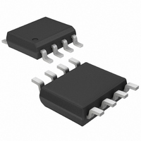
MAX1951ESA+ Maxim Integrated Products, MAX1951ESA+ Datasheet - Page 9

MAX1951ESA+
Manufacturer Part Number
MAX1951ESA+
Description
IC DC-DC PWM SW REG 2A 8-SOIC
Manufacturer
Maxim Integrated Products
Type
Step-Down (Buck)r
Datasheet
1.MAX1952ESA.pdf
(15 pages)
Specifications of MAX1951ESA+
Internal Switch(s)
Yes
Synchronous Rectifier
Yes
Number Of Outputs
1
Voltage - Output
0.8 ~ 5.5 V
Current - Output
2A
Frequency - Switching
1MHz
Voltage - Input
2.6 ~ 5.5 V
Operating Temperature
-40°C ~ 85°C
Mounting Type
Surface Mount
Package / Case
8-SOIC (3.9mm Width)
Power - Output
976mW
Output Voltage
0.8 V
Output Current
2 A
Input Voltage
2.6 V to 5.5 V
Supply Current
6 mA
Switching Frequency
1 MHz
Maximum Operating Temperature
+ 85 C
Minimum Operating Temperature
- 40 C
Lead Free Status / RoHS Status
Lead free / RoHS Compliant
The MAX1951 provides an adjustable output voltage
between 0.8V and V
output. To set the output voltage of the MAX1951 to a
voltage greater than V
to FB and GND using a resistive divider, as shown in
Figure 2a. Choose R2 between 2kΩ and 20kΩ, and set
R3 according to the following equation:
The MAX1951 PWM circuitry is capable of a stable min-
imum duty cycle of 18%. This limits the minimum output
voltage that can be generated to 0.18
may result for V
The MAX1952 provides a preset output voltage.
Connect the output to FB, as shown in Figure 2b.
Use a 2µH inductor with a minimum 2A-rated DC cur-
rent for most applications. For best efficiency, use an
inductor with a DC resistance of less than 20mΩ and a
saturation current greater than 3A (min). See Table 2
for recommended inductors and manufacturers. For
most designs, derive a reasonable inductor value
(L
where f
oscillator. Keep the inductor current ripple percentage
LIR between 20% and 40% of the maximum load cur-
rent for the best compromise of cost, size, and perfor-
mance. Calculate the maximum inductor current as:
Check the final values of the inductor with the output
ripple voltage requirement. The output ripple voltage is
given by:
where ESR is the equivalent series resistance of the
output capacitors.
The input filter capacitor reduces peak currents drawn
from the power source and reduces noise and voltage
ripple on the input caused by the circuit’s switching.
The input capacitor must meet the ripple current
requirement (I
defined by the following equation:
V
L
RIPPLE
INIT
INIT
I
RMS
) from the following equation:
= V
SW
Output Voltage Selection: Adjustable
= V
OUT
=
is the switching frequency (1MHz typ) of the
I
OUT
( /
L(MAX)
1
x (V
(MAX1951) or Preset (MAX1952)
RMS
R3 = R2 x [(V
V
IN
IN
x (V
IN
/V
)
2A PWM Step-Down DC-to-DC Regulators
) imposed by the switching currents
_______________________________________________________________________________________
= (1 + LIR/2) x I
×
OUT
IN
- V
IN
- V
OUT
FB
. Connect FB to output for 0.8V
(
1MHz, All-Ceramic, 2.6V to 5.5V Input,
I
ratios below 0.18.
OUT
OUT
Output Inductor Design
(0.8V typ), connect the output
Input Capacitor Design
)/(V
Design Procedure
OUT
) x ESR / (V
2
IN
×
/V
x LIR x I
V
OUT
FB
OUT(MAX)
) – 1]
×
IN
(
OUT(MAX)
✕
V
IN
x L
V
IN
−
FINAL
. Instability
V
OUT
x f
x f
))
SW
SW
)
)
For duty ratios less than 0.5, the input capacitor RMS
current is higher than the calculated current. Therefore,
use a +20% margin when calculating the RMS current
at lower duty cycles. Use ceramic capacitors for their
low ESR, equivalent series inductance (ESL), and lower
cost. Choose a capacitor that exhibits less than 10°C
temperature rise at the maximum operating RMS cur-
rent for optimum long-term reliability.
After determining the input capacitor, check the input
ripple voltage due to capacitor discharge when the
high-side MOSFET turns on. Calculate the input ripple
voltage as follows:
Keep the input ripple voltage less than 3% of the input
voltage.
The key selection parameters for the output capacitor
are capacitance, ESR, ESL, and the voltage rating
requirements. These affect the overall stability, output
ripple voltage, and transient response of the DC-to-DC
converter. The output ripple occurs due to variations in
the charge stored in the output capacitor, the voltage
drop due to the capacitor’s ESR, and the voltage drop
due to the capacitor’s ESL. Calculate the output voltage
ripple due to the output capacitance, ESR, and ESL as:
where the output ripple due to output capacitance,
ESR, and ESL is:
and I
Use these equations for initial capacitor selection, but
determine final values by testing a prototype or evalua-
tion circuit. As a rule, a smaller ripple current results in
less output voltage ripple. Since the inductor ripple
current is a factor of the inductor value, the output
voltage ripple decreases with larger inductance. Use
ceramic capacitors for their low ESR and ESL at the
switching frequency of the converter. The low ESL of
ceramic capacitors makes ripple voltages negligible.
Load transient response depends on the selected
output capacitor. During a load transient, the output
instantly changes by ESR x I
can respond, the output deviates further, depending on
the inductor and output capacitor values. After a short
time (see the Load Transient Response graph in the
V
V
RIPPLE
RIPPLE(ESL)
P-P
V
I
IN_RIPPLE
P-P
the peak-to-peak inductor current is:
= V
V
= [ (V
RIPPLE(C)
RIPPLE(C)
V
= (I
RIPPLE(ESR)
IN
= (I
whichever is greater
P-P
- V
OUT
= I
/t
OUT
ON
+ V
Output Capacitor Design
P-P
x V
) x ESL or (I
)/f
RIPPLE(ESR)
/(8 x C
OUT
= I
SW
LOAD
P-P
x L) ] x V
)/(f
. Before the controller
OUT
x ESR
SW
P-P
x V
x f
+ V
/t
OUT
SW
IN
OFF
RIPPLE(ESL)
x C
)
/V
) x ESL,
IN
IN
)
9


