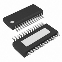
MAX1999EEI+T Maxim Integrated Products, MAX1999EEI+T Datasheet - Page 24

MAX1999EEI+T
Manufacturer Part Number
MAX1999EEI+T
Description
IC CNTRLR PS QUAD HI EFF 28QSOP
Manufacturer
Maxim Integrated Products
Type
Step-Down (Buck)r
Datasheet
1.MAX1977EEIT.pdf
(32 pages)
Specifications of MAX1999EEI+T
Internal Switch(s)
No
Synchronous Rectifier
Yes
Number Of Outputs
4
Voltage - Output
3.3V, 5V, 2 ~ 5.5 V
Current - Output
10A
Frequency - Switching
200kHz, 300kHz, 400kHz, 550kHz
Voltage - Input
6 ~ 24 V
Operating Temperature
-40°C ~ 85°C
Mounting Type
Surface Mount
Package / Case
28-QSOP
Power - Output
860mW
Output Voltage
3.3 V, 2 V to 5.5 V
Input Voltage
6 V to 24 V
Mounting Style
SMD/SMT
Maximum Operating Temperature
+ 85 C
Minimum Operating Temperature
- 40 C
Lead Free Status / RoHS Status
Lead free / RoHS Compliant
High-Efficiency, Quad Output, Main Power-
Supply Controllers for Notebook Computers
below 0.8V clears the overvoltage, undervoltage, and
thermal fault latches.
Connect FB_ to GND to enable the fixed, preset SMPS
output voltages (3.3V and 5V). Connect a resistive volt-
age-divider at FB_ between OUT_ and GND to adjust
the respective output voltage between 2V and 5.5V
(Figure 11). Choose R2 to be about 10kΩ and solve for
R1 using the equation:
where V
When using the adjustable output mode, set the 3.3V
SMPS lower than the 5V SMPS. LDO5 connects to OUT5
through an internal switch only when OUT5 is above the
LDO5 bootstrap-switch threshold (4.56V). LDO3 con-
nects to OUT3 through an internal switch only when
OUT3 is above the LDO3 bootstrap switch threshold
(2.91V). Bootstrapping is most effective when the fixed
output voltages are used. Once LDO_ is bootstrapped
from OUT_, the internal linear regulator turns off. This
reduces internal power dissipation and improves effi-
ciency when LDO_ is powered with a high input voltage.
Figure 11. Setting V
24
______________________________________________________________________________________
MAX1777
MAX1977
MAX1999
FB
= 2V nominal.
OUT_
GND
DH_
DL_
FB_
R
1
OUT_
=
Adjustable-Output Feedback
R
2
with a Resistor-Divider
×
⎛
⎜ ⎜
⎝
V+
V
OUT
V
FB
_
−
1
⎞
⎟ ⎟
⎠
(Dual-Mode FB)
R1
R2
V
OUT_
Establish the input voltage range and maximum load
current before choosing an inductor and its associated
ripple-current ratio (LIR). The following four factors dic-
tate the rest of the design:
1) Input Voltage Range. The maximum value (V+
2) Maximum Load Current. The peak load current
3) Switching Frequency. This choice determines the
4) Inductor Ripple Current Ratio (LIR). LIR is the
must accommodate the maximum AC adapter volt-
age. The minimum value (V+
the lowest input voltage after drops due to connec-
tors, fuses, and battery selector switches. Lower input
voltages result in better efficiency.
ratio of the peak-peak ripple current to the average
inductor current. Size and efficiency trade-offs must
be considered when setting the inductor ripple cur-
rent ratio. Low inductor values cause large ripple
currents, resulting in the smallest size, but poor effi-
ciency and high output noise. The minimum practi-
cal inductor value is one that causes the circuit to
operate at critical conduction (where the inductor
current just touches zero with every cycle at maxi-
mum load). Inductor values lower than this grant no
further size reduction benefit.
The MAX1777/MAX1977/MAX1999s’ pulse-skipping
algorithm (SKIP = GND) initiates skip mode at the
critical conduction point. So the inductor’s operat-
ing point also determines the load current at which
PWM/PFM switchover occurs. The optimum point is
usually found between 20% and 50% ripple current.
(I
nent stress and filtering requirements, and thus dri-
ves output capacitor selection, inductor saturation
rating, and the design of the current-limit circuit.
The continuous load current (I
thermal stress and drives the selection of input
capacitors, MOSFETs, and other critical heat-con-
tributing components.
basic trade-off between size and efficiency. The
optimal frequency is largely a function of maximum
input voltage and MOSFET switching losses. The
MAX1777 has a nominal switching frequency of
200kHz for the 5V SMPS and 300kHz for the 3.3V
SMPS. The MAX1977 has a nominal switching fre-
quency of 400kHz for the 5V SMPS and 500kHz for
the 3.3V SMPS. The MAX1999 has pin-selectable
switching frequency.
LOAD(MAX)
) determines the instantaneous compo-
Design Procedure
(MIN)
LOAD
) must account for
) determines the
(MAX)
)


