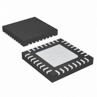
MAX5951ETJ+ Maxim Integrated Products, MAX5951ETJ+ Datasheet - Page 19

MAX5951ETJ+
Manufacturer Part Number
MAX5951ETJ+
Description
IC BUCK PWM CTRLR 12V/5V 32-TQFN
Manufacturer
Maxim Integrated Products
Type
Step-Down (Buck)r
Datasheet
1.MAX5951ETJT.pdf
(25 pages)
Specifications of MAX5951ETJ+
Internal Switch(s)
No
Synchronous Rectifier
No
Number Of Outputs
1
Voltage - Output
0.8 ~ 5.5 V
Current - Output
10A
Frequency - Switching
100kHz ~ 1MHz
Voltage - Input
8 ~ 16 V
Operating Temperature
-40°C ~ 85°C
Mounting Type
Surface Mount
Package / Case
32-TQFN Exposed Pad
Power - Output
2.76W
Lead Free Status / RoHS Status
Lead free / RoHS Compliant
The 32-pin TQFN thermally enhanced package can dis-
sipate 2.7W. Calculate power dissipation in the
MAX5951 as a product of the input voltage and the
total REG output current (I
cent current (I
where Q
low-side and high-side external MOSFETs. f
switching frequency of the converter, and I
escent current of the device at the switching frequency.
Use the following equation to calculate the maximum
power dissipation (P
ent temperature (T
Use the following guidelines to lay out the switching
voltage regulator:
1) Place the IN and DREG bypass capacitors close to
2) Minimize the area and length of the high-current
the MAX5951 PGND pin. Place the REG bypass
capacitor close to the AGND pin.
loops from the input capacitor, upper switching
MOSFET, inductor, and output capacitor back to
the input capacitor negative terminal.
G1
I
REG
and Q
Q
P
) and gate drive current (I
Applications Information
DMAX
= I
A
______________________________________________________________________________________
G2
Q
PC Board Layout Guidelines
):
P
DMAX
D
+ [f
= 34.5 x (150 - T
are the total gate charge of the
= V
SW
) in the chip at a given ambi-
IN
REG
x (Q
x I
PWM Controller
REG
). I
Power Dissipation
12V/5V Input Buck PWM Controller
G1
REG
+ Q
A
includes quies-
G2
)
DREG
)]
Q
is the qui-
SW
):
is the
3) Keep short the current loop formed by the synchro-
4) Keep AGND and PGND isolated and connect them
5) Run the current-sense lines CS+ and CS- close to
6) Avoid long traces between the REG/DREG bypass
7) Place the bank of output capacitors close to the
8) Distribute the power components evenly across the
9) Provide enough copper area at and around the
10) Use 2oz copper to keep the trace inductance and
nous switching MOSFET, inductor, and output
capacitor.
at one single point close to the negative terminal of
the input filter capacitor.
each other to minimize the loop area.
capacitors, driver output of the MAX5951, MOSFET
gates, and PGND. Minimize the loop formed by the
REG bypass capacitors, bootstrap diode, bootstrap
capacitor, the MAX5951, and the upper MOSFET gate.
load.
board for proper heat dissipation.
switching MOSFETs and inductor to aid in thermal
dissipation.
resistance to a minimum. Thin copper PC boards
can compromise efficiency since high currents are
involved in the application. Also, thicker copper
conducts heat more effectively, thereby reducing
thermal impedance.
19


