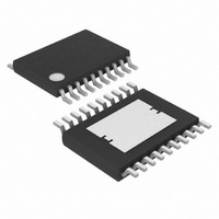
MAX5096AAUP+ Maxim Integrated Products, MAX5096AAUP+ Datasheet - Page 14

MAX5096AAUP+
Manufacturer Part Number
MAX5096AAUP+
Description
IC DC-DC CONV BUCK 20TSSOP
Manufacturer
Maxim Integrated Products
Type
Step-Down (Buck)r
Datasheet
1.MAX5097AATE.pdf
(21 pages)
Specifications of MAX5096AAUP+
Internal Switch(s)
Yes
Synchronous Rectifier
No
Number Of Outputs
2
Voltage - Output
3.3V, 1.24 ~ 11 V
Current - Output
600mA
Frequency - Switching
135kHz
Voltage - Input
5 ~ 40 V
Operating Temperature
-40°C ~ 125°C
Mounting Type
Surface Mount
Package / Case
20-TSSOP Exposed Pad, 20-eTSSOP, 20-HTSSOP
Power - Output
1.74W
Lead Free Status / RoHS Status
Lead free / RoHS Compliant
use typical values of V
mum for typical conditions. The switching frequency (f
is fixed at 135kHz (MAX5096) and 330kHz (MAX5097).
f
(MAX5096) and from 300kHz to 500kHz (MAX5097) when
synchronized to an external clock (see the Oscillator/
Synchronization Input (SYNC) section). The peak-to-peak
inductor current, which reflects the peak-to-peak output
ripple, is worst at the maximum input voltage. See the
Output Capacitor Selection section to verify that the
worst-case output ripple is acceptable. The inductor satu-
rating current (I
current during continuous output short circuit. Select an
inductor with an I
mum peak current limit of 1.9A.
The Buck Mode operation determines the inductor and
output capacitor values. However, the values of the
inductor, its DCR, and the output capacitance/ESR
affect the closed-loop transfer function both in Buck
and LDO Modes. The internal compensation of the
MAX5096/MAX5097 in LDO Mode limits the values of
these external components. Make sure that the combi-
nation of output inductor, capacitor, and ESR falls with-
in the range specified in following Table 1.
40V, 600mA Buck Converters with Low-
Quiescent-Current Linear Regulator Mode
Figure 4. Adjustable Output Voltage Configuration
14
SW
______________________________________________________________________________________
can also be varied from 120kHz to 500kHz
SAT
SAT
) is also important to avoid runaway
IN
specification higher than the maxi-
5V TO 40V
C
C
SS
and f
P
V
IN
100μF
C
IN
SW
C
C
R
C
so that efficiency is opti-
C
CT
EN
SYNC
COMP
SS
CT
V
LDO/BUCK
IN
GND
MAX5096
MAX5097
SW
)
PGND
The allowable output voltage ripple and the maximum
deviation of the output voltage during load steps deter-
mine the output capacitance and its ESR. The output
Table 1. Inductor/Output Capacitor
Selection
RESET
OUT
ADJ
INDUCTOR
BP
LX
100µH
22µH
47µH
D1*
B260/
MURS105
1.0μF
22μH
22µF, ESR = 5mΩ to 20mΩ (ceramic)
47µF, ESR = 40mΩ to 150mΩ
100µF, ESR = 30mΩ to 100mΩ
470µF / ESR = 60Ω to 400mΩ
22µF, ESR = 5mΩ to 20mΩ (ceramic)
47µF / ESR = 40mΩ to 150mΩ
100µF / ESR = 30mΩ to 100mΩ
470µF / ESR = 60mΩ to 400mΩ
22µF, ESR = 5mΩ to 20mΩ (ceramic)
47µF / ESR = 40mΩ to 150mΩ
100µF / ESR = 30mΩ to 100mΩ
470µF / ESR = 60mΩ to 400mΩ
*USE MURS105 IN APPLICATIONS
C
22μF
WHERE LDO MODE QUIESCENT
CURRENT IS CRITICAL.
OUT
Output Capacitor Selection
R
PU
OUTPUT CAPACITOR (C
+
R2
R1
V
RESET
OUT
OUT
)


