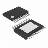
MAX5096AAUP+ Maxim Integrated Products, MAX5096AAUP+ Datasheet - Page 16

MAX5096AAUP+
Manufacturer Part Number
MAX5096AAUP+
Description
IC DC-DC CONV BUCK 20TSSOP
Manufacturer
Maxim Integrated Products
Type
Step-Down (Buck)r
Datasheet
1.MAX5097AATE.pdf
(21 pages)
Specifications of MAX5096AAUP+
Internal Switch(s)
Yes
Synchronous Rectifier
No
Number Of Outputs
2
Voltage - Output
3.3V, 1.24 ~ 11 V
Current - Output
600mA
Frequency - Switching
135kHz
Voltage - Input
5 ~ 40 V
Operating Temperature
-40°C ~ 125°C
Mounting Type
Surface Mount
Package / Case
20-TSSOP Exposed Pad, 20-eTSSOP, 20-HTSSOP
Power - Output
1.74W
Lead Free Status / RoHS Status
Lead free / RoHS Compliant
The MAX5096/MAX5097 in LDO Mode are compensat-
ed internally with a compensation network around the
LDO error amplifier. When in Buck Mode, the DC-DC
g
network connected from COMP to ground. The current-
mode control architecture reduces the compensation
network to a single pole-zero. The RC and C network,
connected from the internal transconductance amplifier
output to SGND, can provide a single pole-zero pair.
Choose all the power components like the inductor,
output capacitor, and ESR first and design the com-
pensation network around them. Choose the closed-
loop bandwidth (f
switching frequency. See the following equations to cal-
culate the compensation values for the low-ESR output
capacitor with ESR zero frequency, approximately a
decade higher than f
Calculate the dominant pole due to the output capaci-
tor (C
where R
Calculate the R
where g
MAX5096/MAX5097 buck converter and is equal to
1.06. V
and g
136µS. See Figure 2.
Place a zero (f
Finally, place a high-frequency pole at the frequency
equal to half of the converter switching frequency (f
Place the compensation network physically close to the
MAX5096/MAX5097.
40V, 600mA Buck Converters with Low-
Quiescent-Current Linear Regulator Mode
16
M
amplifier must be externally compensated using a
______________________________________________________________________________________
OUT
m
ADJ
OUT
(transconductance amplifier gain) is equal to
) and the load (R
MC
R
C
is the feedback set point equal to 1.237V
= V
=
f
is the control to output gain of the
PO
Z
C
g
) at 0.9 x f
OUT
MC
C
using following equation:
=
C
C
2 π
C
×
) to be approximately 1/10 of the
=
C
/ I
× ×
P
R
.
2 π
LOAD
=
OUT
× ×
π
Compensation Network
C
PO
OUT
×
V
OUT
×
O
.
R
:
R
1
g
C
×
CFPO
1
):
m
1
×
f
C
×
×
f
SW
R
V
OUT
ADJ
×
f
PO
×
f
PO
SW
).
The MAX5096/MAX5097 switch between the Buck
Mode and LDO Mode on the fly. However, care must
be taken to reduce output glitch or overshoot during
the switching.
The LDO Mode is intended for the low 100mA output
current while the buck converter delivers up to 600mA
output current. It is important to first reduce the output
load below 100mA before switching to the LDO Mode.
If the output load is higher than 100mA, the
MAX5096/MAX5097 may go into the current limit and
the output will drop significantly. Whenever the mode is
changed, output is expected to glitch because the loop
dynamics change due to different error amplifiers when
operating in the LDO and Buck Modes. The output volt-
age undershoot can be minimized by reducing the out-
put load during switching and using larger output
capacitance.
When switching from the LDO Mode to Buck Mode, a
fixed amount of delay (32 cycles) is applied so that the
buck converter control loop and oscillator reach their
steady-state conditions. The 32-cycle delay translates
to approximately 250µs and 100µs for 150kHz and
330kHz switching frequency versions, respectively. It is
recommended that the output load of 600mA must be
delayed by at least this much time to allow the
MAX5096/MAX5097 to switch to high-current Buck
Mode. This ensures that the output does not drop due
to the LDO current-limit protection mechanism.
1) Proper PC board layout is essential. Minimize
2) Minimize lead lengths to reduce stray capacitance,
ground noise by connecting the anode of the free-
wheeling rectifier, the input bypass capacitor
ground lead, and the output filter capacitor ground
lead to a large PGND plane.
trace resistance, and radiated noise. In particular,
place the Schottky/fast recovery rectifier diode right
next to the device.
PC Board Layout Guidelines
Switching Between LDO Mode
Buck Mode to LDO Mode
LDO Mode to Buck Mode
and Buck Mode


