NCP3101BMNTXG ON Semiconductor, NCP3101BMNTXG Datasheet - Page 15
NCP3101BMNTXG
Manufacturer Part Number
NCP3101BMNTXG
Description
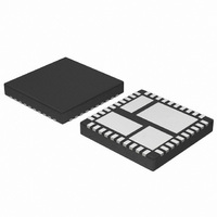
IC CONV VOLT SYNC BUCK 6A 40-QFN
Manufacturer
ON Semiconductor
Type
Step-Down (Buck)r
Datasheet
1.NCP3101BMNTXG.pdf
(26 pages)
Specifications of NCP3101BMNTXG
Internal Switch(s)
Yes
Synchronous Rectifier
Yes
Number Of Outputs
1
Voltage - Output
Adj to 0.8V
Current - Output
6A
Frequency - Switching
275kHz
Voltage - Input
4.5 ~ 13.2 V
Operating Temperature
-40°C ~ 85°C
Mounting Type
Surface Mount
Package / Case
40-TQFN Exposed Pad
Power - Output
3W
Lead Free Status / RoHS Status
Lead free / RoHS Compliant


Input Capacitor Selection
produced during the on time of the upper MOSFET,
therefore must have a low ESR to minimize losses. The
RMS value of the input ripple current is:
D
IIN
I
Loss in the input capacitors can be calculated with the
following equation:
CIN
OUT
Table 5. TRANSIENT RESPONSE VERSUS OUTPUT
CAPACITANCE
Figure 27. Typical Waveform of Transient Response
IIN
2.68 A + 6.0 A 27.5%
71.8 mW + 10 mW
The input capacitor has to sustain the ripple current
The equation reaches its maximum value with D = 0.5.
RMS
COUT OS−CON (mF)
ESR
RMS
P
CIN
+ I
+ CIN
1000
100
150
220
270
560
820
OUT
0
= Duty ratio
= Input capacitance RMS current
= Load current
= Input capacitance Equivalent Series
ESR
(50% to 100% Load Step)
Resistance
D
2.68 A
IIN
1 * D ³
1 * 27.5%
RMS
2
Drop
(mV)
384
224
192
164
156
128
112
112
2
Recovery Time
(ms)
336
298
278
238
212
198
118
116
(eq. 19)
(eq. 20)
http://onsemi.com
15
IIN
P
or ceramics should be used. If a tantalum capacitor must be
used, it must be surge protected, otherwise capacitor failure
could occur.
Power MOSFET Dissipation
environment drive power supply design. Once the
dissipation is known, the thermal impedance can be
calculated to prevent the specified maximum junction
temperatures from being exceeded at the highest ambient
temperature.
conduction losses and switching losses. The high−side
MOSFET will display both switching and conduction
losses. The switching losses of the low side MOSFET will
not be calculated as it switches into nearly zero voltage and
the losses are insignificant. However, the body diode in the
low−side MOSFET will suffer diode losses during the
non−overlap time of the gate drivers.
dissipation can be approximated from:
P
P
P
high−side MOSFET while it is on.
I
R
P
Using the ra term from Equation 5, I
D
ra
I
I
The second term from Equation 21 is the total switching loss
and can be approximated from the following equations.
P
P
P
RMS_HS
OUT
RMS_HS
CIN
COND
D_HS
SW_TOT
COND
DS
RR
SW
P
DS(ON)_HS
Due to large di/dt through the input capacitors, electrolytic
Power dissipation, package size, and the thermal
Power dissipation has two primary contributors:
Starting with the high−side MOSFET, the power
The first term in Equation 21 is the conduction loss of the
D_HS
RMS
= Conduction power losses
+ P
= RMS current in the high side MOSFET
I
P
COND
= On resistance of the high side MOSFET
RMS_HS
COND
P
SW_TOT
= Input capacitance RMS current
= Power loss in the input capacitor
= Conduction losses
= Power losses in the high side MOSFET
= Total switching losses
= Duty ratio
= Ripple current ratio
= Output current
= High side MOSFET RMS current
= High side MOSFET drain to source
= High side MOSFET reverse recovery
= High side MOSFET switching losses
) P
losses
losses
+ I
+ I
SW_TOT
+ P
RMS_HS
OUT
SW
@
) P
2
D @ 1 )
@ R
DS
RMS
DS(on)_HS
) P
becomes:
ra
RR
12
2
(eq. 21)
(eq. 22)
(eq. 23)
(eq. 24)
Related parts for NCP3101BMNTXG
Image
Part Number
Description
Manufacturer
Datasheet
Request
R

Part Number:
Description:
Wide Input Voltage Synchronous Buck Converter
Manufacturer:
ON Semiconductor
Datasheet:
Part Number:
Description:
ON Semiconductor [VOLTAGE REGULATOR]
Manufacturer:
ON Semiconductor
Datasheet:
Part Number:
Description:
357-036-542-201 CARDEDGE 36POS DL .156 BLK LOPRO
Manufacturer:
ON Semiconductor
Datasheet:
Part Number:
Description:
357-036-542-201 CARDEDGE 36POS DL .156 BLK LOPRO
Manufacturer:
ON Semiconductor
Datasheet:
Part Number:
Description:
357-036-542-201 CARDEDGE 36POS DL .156 BLK LOPRO
Manufacturer:
ON Semiconductor
Datasheet:
Part Number:
Description:
357-036-542-201 CARDEDGE 36POS DL .156 BLK LOPRO
Manufacturer:
ON Semiconductor
Datasheet:
Part Number:
Description:
357-036-542-201 CARDEDGE 36POS DL .156 BLK LOPRO
Manufacturer:
ON Semiconductor
Datasheet:
Part Number:
Description:
357-036-542-201 CARDEDGE 36POS DL .156 BLK LOPRO
Manufacturer:
ON Semiconductor
Datasheet:
Part Number:
Description:
357-036-542-201 CARDEDGE 36POS DL .156 BLK LOPRO
Manufacturer:
ON Semiconductor
Datasheet:
Part Number:
Description:
357-036-542-201 CARDEDGE 36POS DL .156 BLK LOPRO
Manufacturer:
ON Semiconductor
Datasheet:
Part Number:
Description:
357-036-542-201 CARDEDGE 36POS DL .156 BLK LOPRO
Manufacturer:
ON Semiconductor
Datasheet:
Part Number:
Description:
357-036-542-201 CARDEDGE 36POS DL .156 BLK LOPRO
Manufacturer:
ON Semiconductor
Datasheet:
Part Number:
Description:
Manufacturer:
ON Semiconductor
Datasheet:
Part Number:
Description:
Manufacturer:
ON Semiconductor
Datasheet: