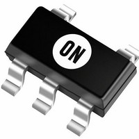
NCP1450ASN27T1G ON Semiconductor, NCP1450ASN27T1G Datasheet - Page 17

NCP1450ASN27T1G
Manufacturer Part Number
NCP1450ASN27T1G
Description
IC CTRLR DC-DC PWM 2.7V SOT23-5
Manufacturer
ON Semiconductor
Type
Step-Up (Boost), Inverting, Flyback, Forward Converter, Sepicr
Datasheet
1.NCP1450ASN19T1.pdf
(22 pages)
Specifications of NCP1450ASN27T1G
Internal Switch(s)
No
Synchronous Rectifier
No
Number Of Outputs
1
Voltage - Output
2.7V
Current - Output
1A
Frequency - Switching
180kHz
Voltage - Input
0.6 ~ 5.5 V
Operating Temperature
-40°C ~ 85°C
Mounting Type
Surface Mount
Package / Case
TSOT-23-5, TSOT-5, TSOP-5
Power - Output
500mW
Mounting Style
SMD/SMT
Lead Free Status / RoHS Status
Lead free / RoHS Compliant
Other names
NCP1450ASN27T1GOS
NCP1450ASN27T1GOS
NCP1450ASN27T1GOSTR
NCP1450ASN27T1GOS
NCP1450ASN27T1GOSTR
Available stocks
Company
Part Number
Manufacturer
Quantity
Price
Company:
Part Number:
NCP1450ASN27T1G
Manufacturer:
ON Semiconductor
Quantity:
2 200
Part Number:
NCP1450ASN27T1G
Manufacturer:
ON/安森美
Quantity:
20 000
Operation
controllers optimized for battery powered portable products
where large output current is required.
voltage−mode PWM DC−DC controllers, and consist of
startup circuit, feedback resistor divider, reference voltage,
oscillator, loop compensation network, PWM control
circuit, and low ON resistance driver. Due to the on−chip
feedback resistor and loop compensation network, the
system designer can get the regulated output voltage from
1.8 V to 5.0 V with 0.1 V stepwise with a small number of
external components. The quiescent current is typically
93 mA (V
reduced to about 1.5 mA when the chip is disabled (V
0.3 V).
referring to the block diagram in Figure 2. The error
amplifier monitors the output voltage via the feedback
resistor divider by comparing the feedback voltage with the
reference voltage. When the feedback voltage is lower than
the reference voltage, the error amplifier output will
decrease. The error amplifier output is then compared with
the oscillator ramp voltage at the PWM controller. When the
ramp voltage is higher than the error amplifier output, the
high−side driver is turned on and the low−side driver is
turned off which will then switch on the external transistor;
and vice versa. As the error amplifier output decreases, the
high−side driver turn−on time increases and duty cycle
increases. When the feedback voltage is higher than the
reference voltage, the error amplifier output increases and
the duty cycle decreases. When the external power switch is
on, the current ramps up in the inductor, storing energy in the
magnetic field. When the external power switch is off, the
energy stored in the magnetic field is transferred to the
output filter capacitor and the load. The output filter
capacitor stores the charge while the inductor current is
higher than the output current, then sustains the output
voltage until the next switching cycle.
on for a shorter duty cycle. Under the light load condition,
the controller will skip switching cycles to reduce power
consumption, so that high efficiency is maintained at light
loads.
The NCP1450A series are monolithic power switching
The NCP1450A series are low noise fixed frequency
The NCP1450A operation can be best understood by
As the load current is decreased, the switch transistor turns
OUT
= 2.7 V, f
OSC
= 180 kHz), and can be further
DETAILED OPERATING DESCRIPTION
http://onsemi.com
CE
NCP1450A
t
17
Soft Start
applied to the device, the soft start circuit first pumps up the
output voltage to approximately 1.5 V at a fixed duty cycle.
This is the voltage level at which the controller can operate
normally. In addition to that, the startup capability with
heavy loads is also improved.
Oscillator
accuracy of "20% and with low temperature coefficient of
0.11%/°C.
Regulated Converter Voltage (V
network. This is trimmed to a selected voltage from 1.8 V to
5.0 V range in 100 mV steps with an accuracy of "2.5%.
Compensation
conduction mode. An internal compensation circuit was
designed to guarantee stability over the full input/output
voltage and full output load range.
Enable/Disable Operation
enable pin (CE pin) to reduce current consumption. When
voltage at pin CE is equal or greater than 0.9 V, the chip will
be enabled, which means the controller is in normal
operation. When voltage at pin CE is less than 0.3 V, the chip
is disabled, which means IC is shutdown.
Important: DO NOT apply a voltage between 0.3 V to 0.9 V
to pin CE as this is the CE pin’s hysteresis voltage range.
Clearly defined output states can only be obtained by
applying voltage out of this range.
There is a soft start circuit in NCP1450A. When power is
The oscillator frequency is internally set to 180 kHz at an
The V
The device is designed to operate in continuous
The NCP1450A series offer IC shutdown mode by chip
OUT
is set by an integrated feedback resistor
OUT
)


