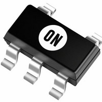
NCP1450ASN27T1G ON Semiconductor, NCP1450ASN27T1G Datasheet - Page 19

NCP1450ASN27T1G
Manufacturer Part Number
NCP1450ASN27T1G
Description
IC CTRLR DC-DC PWM 2.7V SOT23-5
Manufacturer
ON Semiconductor
Type
Step-Up (Boost), Inverting, Flyback, Forward Converter, Sepicr
Datasheet
1.NCP1450ASN19T1.pdf
(22 pages)
Specifications of NCP1450ASN27T1G
Internal Switch(s)
No
Synchronous Rectifier
No
Number Of Outputs
1
Voltage - Output
2.7V
Current - Output
1A
Frequency - Switching
180kHz
Voltage - Input
0.6 ~ 5.5 V
Operating Temperature
-40°C ~ 85°C
Mounting Type
Surface Mount
Package / Case
TSOT-23-5, TSOT-5, TSOP-5
Power - Output
500mW
Mounting Style
SMD/SMT
Lead Free Status / RoHS Status
Lead free / RoHS Compliant
Other names
NCP1450ASN27T1GOS
NCP1450ASN27T1GOS
NCP1450ASN27T1GOSTR
NCP1450ASN27T1GOS
NCP1450ASN27T1GOSTR
Available stocks
Company
Part Number
Manufacturer
Quantity
Price
Company:
Part Number:
NCP1450ASN27T1G
Manufacturer:
ON Semiconductor
Quantity:
2 200
Part Number:
NCP1450ASN27T1G
Manufacturer:
ON/安森美
Quantity:
20 000
Diode
converters. The most importance parameters which affect
their efficiency are the forward voltage drop, V
reverse recovery time, trr. The forward voltage drop creates
a loss just by having a voltage across the device while a
current flowing through it. The reverse recovery time
generates a loss when the diode is reverse biased, and the
current appears to actually flow backwards through the
diode due to the minority carriers being swept from the P−N
junction.
characteristics is recommended:
Input Capacitor
minimize peak current ripple from the source. The value of
the capacitor depends on the impedance of the input source
used. Small Equivalent Series Resistance (ESR) Tantalum
or ceramic capacitor with a value of 10 mF should be
suitable.
Output Capacitor
voltage when the external MOSFET or bipolar transistor is
switched on and smoothing the ripple voltage. Low ESR
capacitor should be used to reduce output ripple voltage. In
general, a 100 mF to 220 mF low ESR (0.10 W to 0.30 W)
Tantalum capacitor should be appropriate.
External Switch Transistor
transistor can be used as the external switch transistor.
enhancement MOSFET is a voltage driven device, it is a
External Component Reference Data
NCP1450ASN19T1
NCP1450ASN30T1
NCP1450ASN50T1
NCP1450ASN19T1
NCP1450ASN30T1
NCP1450ASN50T1
The diode is the largest source of loss in DC−DC
The input capacitor can stabilize the input voltage and
The output capacitor is used for sustaining the output
An enhancement N−channel MOSFET or a bipolar NPN
For
Small forward voltage, V
Small reverse leakage current
Fast reverse recovery time/switching speed
Rated current larger than peak inductor current,
Reverse voltage larger than output voltage,
I
V
rated
reverse
Device
enhancement
u I
A
u V
PK
Schottky
OUT
N−channel
diode
F
V
1.9 V
3.0 V
5.0 V
1.9 V
3.0 V
5.0 V
t 0.3 V
OUT
with
MOSFET,
the
Inductor
Model
CD54
CD54
CD54
CD54
CD54
CD54
D
following
, and the
http://onsemi.com
since
NCP1450A
19
Inductor
more efficient switch than a BJT transistor. However, the
MOSFET requires a higher voltage to turn on as compared
with BJT transistors. An enhancement N−channel MOSFET
can be selected by the following guidelines:
continuous collector current typically 1 A to 5 A and V
< 0.2 V should be employed. The driving capability is
determined by the DC current gain, H
the base resistor, Rb; and the controller’s EXT pin must be
able to supply the necessary driving current.
Rb can be calculated by the following equation:
exact Rb value should be finely tuned by the experiment.
Generally, a small Rb value can increase the output current
capability, but the efficiency will decrease due to more
energy is used to drive the transistor.
in parallel with Rb to reduce switching loss and improve
efficiency. Cb can be calculated by the equation below:
transistor used. The calculated value should be used as the
initial test value and the optimized value should be obtained
by the experiment.
Value
12 mH
10 mH
10 mH
12 mH
10 mH
10 mH
For bipolar NPN transistor, medium power transistor with
Since the pulse current flows through the transistor, the
Moreover, a speed−up capacitor, Cb, should be connected
It is due to the variation in the characteristics of the
1. Low ON−resistance, R
2. Low gate threshold voltage, V
3. Rated continuous drain current, I
4. Gate capacitance should be 1200 pF or less.
V
for the low V
larger than the peak inductor current, i.e. I
OUT
, typically < 1.5 V, it is especially important
Rb +
Cb v
NTGS3446T1
NTGS3446T1
NTGS3446T1
MMJT9410
MMJT9410
MMJT9410
Transistor
External
V OUT * 0.7
2p
OUT
Ib +
device, like V
Ib
Rb
H FE
I PK
DS(on)
MBRM110L
MBRM110L
MBRM110L
MBRM110L
MBRM110L
MBRM110L
1
f OSC
*
Diode
, typically < 0.1 W.
| I EXTH |
FE
GS(th)
, of the transistor and
0.4
OUT
D
0.7
, should be
, must be <
= 1.9 V.
Capacitor
Output
220 mF
220 mF
220 mF
220 mF
220 mF
220 mF
D
> I
CE(sat)
PK
.


