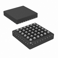
LM8322JGR8/NOPB National Semiconductor, LM8322JGR8/NOPB Datasheet - Page 13

LM8322JGR8/NOPB
Manufacturer Part Number
LM8322JGR8/NOPB
Description
IC MOBILE I/O COMPAN 36MICRARRAY
Manufacturer
National Semiconductor
Datasheet
1.LM8322JGR8NOPB.pdf
(42 pages)
Specifications of LM8322JGR8/NOPB
Applications
*
Mounting Type
Surface Mount
Package / Case
36-Micro Array
For Use With
LM8322EVALKIT - BOARD EVALUATION LM8322
Lead Free Status / RoHS Status
Lead free / RoHS Compliant
Other names
LM8322JGR8
LM8322JGR8TR
LM8322JGR8TR
Available stocks
Company
Part Number
Manufacturer
Quantity
Price
Company:
Part Number:
LM8322JGR8/NOPB
Manufacturer:
National Semiconductor
Quantity:
135
10.7 INITIALIZATION EXAMPLE
In the following example, the LM8322 is configured as:
•
•
•
•
•
•
•
11.0 Halt Mode
The fully static architecture of the LM8322 allows stopping the
internal RC clock in Halt mode, which reduces power con-
sumption to the minimum level. Figure 6 shows the current in
Halt mode at the maximum V
WRITE_PORT_STATE
Keypad matrix configuration is 8 × 4.
GPIO_03 through GPIO_07 are available to use as GPIO
pins.
GPIO_03 is an output driven low.
GPIO_4 and GPIO_5 are outputs driven high.
GPIO_06 and GPIO_07 are inputs with weak pulldowns.
GPIO_14 and GPIO_15 are inputs with weak pullups.
The PWM clock source is the internal execution clock
divided by 64 (about 32 kHz).
WRITE_PULL_DOWN
FIGURE 6. Halt Current vs. Temperature at 1.98V
WRITE_PORT_SEL
SET_DEBOUNCE
SET_KEY_SIZE
SET_ACTIVE
WRITE_CFG
WRITE_CLK
Command
CC
Encoding Parameter 1 Parameter 2
(1.98V) from 25°C to +85°C.
0x8B
0x81
0x93
0x90
0x8F
0x85
0x84
0x86
0xC0
0x40
0x08
0x84
0x4B
0x03
0x00
0x00
30013606
0x38
0x3F
0xF0
13
Most of these settings can be verified by executing com-
mands
READ_CLOCK, etc.
ALL
READ_PORT_STATE command, without regard to whether
the pin is an input or an output.
An open-drain signal can be created by alternating between
input mode and driving the output low.
All GPIO s can sink and source 16 mA when configured as
an output.
Halt mode is entered when no key-press event, key-release
event, or ACCESS.bus activity is detected for a certain period
of time (by default, 500 milliseconds). The mechanism for en-
tering Halt mode is always enabled in hardware, but the host
can program the period of inactivity which triggers entry into
Halt mode.
11.1 ACCESS.bus ACTIVITY
When the LM8322 is in Halt mode, any activity on the
ACCESS.bus interface will cause the LM8322 to exit from
Halt mode. However, the LM8322 will not be able to acknowl-
edge the first bus cycle immediately following wake-up from
Halt mode. It will respond with a negative acknowledgement,
and the host should then repeat the cycle.
The LM8322 will be prevented from entering Halt mode if it
shares the bus with peripherals that are continuously active.
For lowest power consumption, the LM8322 should only
share the bus with peripherals that require little or no bus ac-
tivity after system initialization.
Selects 36-pin package and disables the two digital
multiplexers.
SLOWCLKOUT disabled, no external 32.768 kHz clock
required, PWM clock source is internal.
Selects a keypad matrix size of 8 × 4.
Sets the active time to about 300 milliseconds (75 × 4
milliseconds).
Sets the key debouncing time to about 12 milliseconds
(3 × 4 ms). This is actually the default and would not have
to be performed.
Configure GPIO_03, GPIO_04, and GPIO_05 as
outputs. Configure GPIO_06, GPIO_07, GPIO_14, and
GPIO_15 as inputs.
Set the direction for the pullup/pulldown devices on
GPIO_06 and GPIO_07 to pulldown. Set the direction for
the pullup/pulldown devices on GPIO_14 and GPIO_15
to pullup.
Set GPIO_04 and GPIO_05 to drive high. Enable the
pullups on GPIO_06, GPIO_07, GPIO_14, and
GPIO_15.
GPIO
such
pin
as
states
READ_CONF,
Description
can
be
READ_PORT_SEL,
read
www.national.com
using
the


