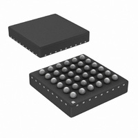
LM8322JGR8/NOPB National Semiconductor, LM8322JGR8/NOPB Datasheet - Page 38

LM8322JGR8/NOPB
Manufacturer Part Number
LM8322JGR8/NOPB
Description
IC MOBILE I/O COMPAN 36MICRARRAY
Manufacturer
National Semiconductor
Datasheet
1.LM8322JGR8NOPB.pdf
(42 pages)
Specifications of LM8322JGR8/NOPB
Applications
*
Mounting Type
Surface Mount
Package / Case
36-Micro Array
For Use With
LM8322EVALKIT - BOARD EVALUATION LM8322
Lead Free Status / RoHS Status
Lead free / RoHS Compliant
Other names
LM8322JGR8
LM8322JGR8TR
LM8322JGR8TR
Available stocks
Company
Part Number
Manufacturer
Quantity
Price
Company:
Part Number:
LM8322JGR8/NOPB
Manufacturer:
National Semiconductor
Quantity:
135
www.national.com
V
I
I
V
V
C
Symbo
DD
HALT
CC
IL
IH
PAD
18.0 Absolute Maximum Ratings
1)
If Military/Aerospace specified devices are required,
please contact the National Semiconductor Sales Office/
Distributors for availability and specifications.
19.0 DC Electrical Characteristics
(Temperature: -40°C
Data sheet specification limits are guaranteed by design, test, or statistical analysis.
Note 1: Absolute Maximum Ratings indicate limits beyond which damage to the device may occur. Operating Ratings indicate conditions for which the device is
intended to be functional, but specific performance is not guaranteed. For guaranteed specifications and test conditions, see the Electrical Characteristics tables.
Note 2: Supply current is measured with inputs connected to V
Note 3: T
Note 4: In standby mode, the internal clock is switched off. Supply current in standby mode is measured with inputs connected to V
not connected to a load.
Note 5: Applied to all digital pins (including RESET) except for SLOWCLK when configured for an external clock..
Note 6: Guaranteed by design, not tested.
Note 7: The sum of all I/O sink/source current must not e4xceed the maximum total current into V
ratings.
Supply Voltage (V
Voltage at Any Pin
Maximum Input Current Without
Latchup
l
Operating Voltage
Supply Current (Note 2)
Standby Mode Current (Note 5)
Logical 0 Input Voltage (Note 5)
Logical 1 Input Voltage (Note 5)
Hi-Z Input Leakage (TRI-STATE Output)
Port Input Hysteresis (Notes 5, 6)
Weak Pull-Up/Pull-Down Current
Output Current Source (Push-Pull Mode)
Output CurrentSink (Push-Pull Mode)
Allowable Sink and Source Current per Pin (Note
7)
Input Capacitance (Note 7)
C
= instruction cycle time (min. 0.7 µs).
CC
≤
)
T
A
Parameter
≤
+85°C)
-0.3V to V
±100 mA
CC
CC
+0.3V
and outputs driven low but not connected to a load.
(Note
2V
Internal Clock,
No loads on pins,
V
Typical:
V
V
1.6V<V
V
V
CC
CC
CC
CC
CC
= 1.9V, T
= 1.9V, T
= 1.8V
= 1.62V, V
= 1.62V, V
38
CC
< 2.0V
Conditions
ESD Protection Level
(Human Body Model)
(Machine Model)
(Charge Device Model)
Total Current into V
Total Current out of GND Pin (Sink)
Storage Temperature Range
C
A
OH
OL
= 25°C
= 0.5µs (Note 4)
= 0.3 x V
= 0.7 x V
CC
and out of GND as specified in the absolute maximem
CC
CC
CC
Pin (Source)
0.3 x V
1.62
Min
100
16
-2
CC
Typ
400
CC
1.9
<9
and outputs driven low but
−65°C to +140°C
0.7 x V
Max
1.98
150
3.0
-16
40
16
2
5
100 mA
100 mA
CC
200V
750V
2 kV
Units
mA
mA
mA
mA
mA
µA
µA
µA
pF
V
V
V


