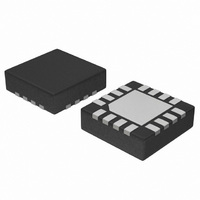
NBSG16MMNR2G ON Semiconductor, NBSG16MMNR2G Datasheet - Page 4

NBSG16MMNR2G
Manufacturer Part Number
NBSG16MMNR2G
Description
IC RCVR/DRVR CML 2.5/3.3V 16-QFN
Manufacturer
ON Semiconductor
Type
Transceiverr
Datasheet
1.NBSG16MMNR2G.pdf
(11 pages)
Specifications of NBSG16MMNR2G
Applications
Instrumentation
Mounting Type
Surface Mount
Package / Case
16-TFQFN Exposed Pad
Logic Family
NBSG
Logic Type
Receiver and Driver Translator Buffer
Supply Voltage (max)
3.465 V, - 3.465 V
Supply Voltage (min)
2.375 V, - 2.375 V
Maximum Operating Temperature
+ 85 C
Mounting Style
SMD/SMT
Data Rate
10000 Mbps
Minimum Operating Temperature
- 40 C
Supply Current
51 mA
Lead Free Status / RoHS Status
Lead free / RoHS Compliant
Table 4. MAXIMUM RATINGS
Symbol
Stresses exceeding Maximum Ratings may damage the device. Maximum Ratings are stress ratings only. Functional operation above the
Recommended Operating Conditions is not implied. Extended exposure to stresses above the Recommended Operating Conditions may
affect device reliability.
5. JEDEC standard multilayer board − 1S2P (1 signal, 2 power)
V
V
V
V
I
I
I
T
T
q
q
T
IN
out
BB
A
stg
JA
JC
sol
CC
EE
I
INPP
Positive Power Supply
Negative Power Supply
Positive Input
Negative Input
Differential Input Voltage |D − D|
Input Current Through R
Output Current
V
Operating Temperature Range
Storage Temperature Range
Thermal Resistance (Junction−to−Ambient)
(Note 5)
Thermal Resistance (Junction−to−Case)
Wave Solder
BB
Sink/Source
Parameter
T
(50 W Resistor)
Pb−Free
Pb
http://onsemi.com
V
V
V
V
V
V
Static
Surge
Continuous
Surge
0 lfpm
500 lfpm
1S2P (Note 5)
<2 to 3 sec @ 248°C
<2 to 3 sec @ 260°C
EE
CC
EE
CC
CC
CC
= 0 V
= 0 V
= 0 V
= 0 V
− V
− V
Condition 1
EE
EE
4
w 2.8 V
< 2.8 V
V
V
QFN−16
QFN−16
QFN−16
I
I
v V
w V
Condition 2
CC
EE
−65 to +150
|V
−40 to +85
CC
Rating
−3.6
−3.6
265
265
3.6
3.6
2.8
1.0
4.0
45
80
25
50
42
35
− V
EE
|
°C/W
°C/W
°C/W
Unit
mA
mA
mA
mA
mA
°C
°C
°C
V
V
V
V
V


