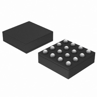
NBSG16VSBAHTBG ON Semiconductor, NBSG16VSBAHTBG Datasheet

NBSG16VSBAHTBG
Specifications of NBSG16VSBAHTBG
Available stocks
Related parts for NBSG16VSBAHTBG
NBSG16VSBAHTBG Summary of contents
Page 1
NBSG16VS 2.5V/3.3V SiGe Differential Receiver/Driver with Variable Output Swing Description The NBSG16VS is a differential receiver/driver targeted for high frequency applications that require variable output swing. The device is functionally equivalent to the EP16VS device with much higher bandwidth and lower ...
Page 2
CTRL VTD VTD Figure 1. BGA−16 Pinout (Top View) Table ...
Page 3
0.1 mF CTRL V V CTRL CC V VTD 36 VTD V EE Figure 3. Logic Diagram/ Voltage Source Implementation Table 2. ...
Page 4
Table 3. ATTRIBUTES Internal Input Pulldown Resistor (D, D) Internal Input Pullup Resistor (D) ESD Protection Moisture Sensitivity (Note 4) Flammability Rating Transistor Count Meets or exceeds JEDEC Spec EIA/JESD78 IC Latchup Test 4. For additional information, see Application Note ...
Page 5
Table 5. DC CHARACTERISTICS, INPUT WITH VARIABLE PECL OUTPUT Symbol Characteristic I Negative Power Supply Current EE V Output HIGH Voltage (Note Output LOW Voltage (Note CTRL CC V Input HIGH Voltage ...
Page 6
Table 6. DC CHARACTERISTICS, INPUT WITH VARIABLE PECL OUTPUT Symbol Characteristic I Negative Power Supply Current EE V Output HIGH Voltage (Note 13 Output LOW Voltage (Note 13 CTRL CC V Input HIGH Voltage ...
Page 7
Table 7. DC CHARACTERISTICS, NECL INPUT WITH VARIABLE NECL OUTPUT −3.465 V to −2.375 V (Note 19 Symbol Characteristic I Negative Power Supply Current EE V Output HIGH Voltage (Note 20) OH ...
Page 8
Table 8. AC CHARACTERISTICS for FCBGA−16 Symbol Characteristic f Maximum Frequency max (See Figure 8) (Note 26 Propagation Delay to Output Differen- PLH t tial PHL ( − → CTRL CC ...
Page 9
Table 10. AC CHARACTERISTICS for QFN−16 Symbol Characteristic f Maximum Frequency max (See Figure 8) (Note 34 Propagation Delay to PLH t Output Differential PHL ( − → CTRL CC (V ...
Page 10
V − 0.0 V − 0 Figure 5. Output Amplitude % vs MIN. AMPLITUDE REGION − 0.0 V − 0.5 CC ...
Page 11
OUTPUT P−P SPEC 300 (AMPLITUDE GUARANTEE) 200 100 Figure 8. Output Voltage Amplitude (V (Typical) See Tables 8 and 800 700 600 500 400 OUTPUT P−P SPEC ...
Page 12
... Q Driver Device Q Figure 11. Typical Termination for Output Driver and Device Evaluation (See Application Note AND8020/D − Termination of ECL Logic Devices.) ORDERING INFORMATION Device NBSG16VSBAHTBG NBSG16VSBA NBSG16VSBAR2 NBSG16VSMN NBSG16VSMNG NBSG16VSMNR2 NBSG16VSMNR2G NBSG16VSMNHTBG Board NBSG16VSBAEVB †For information on tape and reel specifications, including part orientation and tape sizes, please refer to our Tape and Reel Packaging Specifications Brochure, BRD8011/D ...
Page 13
PLASTIC 4X4 (mm) BGA FLIP CHIP PACKAGE LASER MARK FOR PIN 1 IDENTIFICATION IN −X− THIS AREA D −Y− VIEW M− DETAIL K _ ROTATED 90 ...
Page 14
... Pb−Free strategy and soldering details, please download the ON Semiconductor Soldering and Mounting Techniques Reference Manual, SOLDERRM/D. N. American Technical Support: 800−282−9855 Toll Free USA/Canada Europe, Middle East and Africa Technical Support: Phone: 421 33 790 2910 Japan Customer Focus Center Phone: 81− ...


