NBSG16VSBAHTBG ON Semiconductor, NBSG16VSBAHTBG Datasheet - Page 2
NBSG16VSBAHTBG
Manufacturer Part Number
NBSG16VSBAHTBG
Description
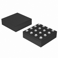
IC RX/DRIVER SIGE DIFF 16-BGA
Manufacturer
ON Semiconductor
Type
Transceiverr
Datasheet
1.NBSG16VSMNR2G.pdf
(14 pages)
Specifications of NBSG16VSBAHTBG
Applications
Instrumentation
Mounting Type
Surface Mount
Package / Case
16-FCBGA
Lead Free Status / RoHS Status
Lead free / RoHS Compliant
Available stocks
Company
Part Number
Manufacturer
Quantity
Price
Company:

Part Number:
NBSG16VSBAHTBG
Manufacturer:
ON Semiconductor
Quantity:
10 000


Table 1. PIN DESCRIPTION
1. The NC pin is electrically connected to the die and must be left open.
2. All V
3. In the differential configuration when the input termination pins (VTD, VTD) are connected to a common termination voltage, and if no signal
A1,D1,A4,
C
D
A
B
B3,C3
BGA
bottom (see case drawing) must be attached to a heat−sinking conduit.
is applied then the device will be susceptible to self−oscillation.
N/A
C2
C1
B1
B2
D4
A2
A3
B4
C4
D3
D2
Figure 1. BGA−16 Pinout (Top View)
CC
V
V
D
D
and V
EE
EE
Pin
1
5,8,13,16
EE
QFN
9,12
VTD
VTD
V
10
11
14
15
NC
1
2
3
4
6
7
−
pins must be externally connected to Power Supply to guarantee proper operation. The thermally exposed pad on package
BB
2
V
V
V
V
CTRL
MM
CC
CC
3
Name
V
VTD
VTD
V
V
V
V
NC
CTRL
EP
Q
Q
D
D
MM
CC
EE
BB
V
V
4
Q
Q
EE
EE
ECL, CML,
ECL, CML,
LVCMOS,
LVCMOS,
RSECL
RSECL
LVTTL
LVTTL
Output
Output
LVDS,
LVDS,
Input
Input
I/O
−
−
−
−
−
−
−
−
Internal 50 W Termination Pin. See Table 2.
Inverted Differential Input. Internal 75 kW to V
Noninverted Differential Input. Internal 75 kW to V
Internal 50 W Termination Pin. See Table 2.
Negative Supply Voltage
No Connect
Output Amplitude Swing Control. Bypass Pin to V
Positive Supply Voltage
Noninverted Differential Output. Typically Terminated with 50 W to
V
Inverted Differential Output. Typically Terminated with 50 W to V
LVCMOS Reference Voltage Output. (V
ECL Reference Voltage Output
The Exposed Pad (EP) and the QFN−16 package bottom is thermally connected
to the die for improved heat transfer out of package. The exposed pad must be
attached to a heat−sinking conduit. The pad is not electrically connected to the
die but may be electrically and thermally connected to V
http://onsemi.com
TT
= V
CC
− 2 V
2
VTD
VTD
D
D
Figure 2. QFN−16 Pinout (Top View)
1
2
3
4
V
V
16
EE
EE
5
NBSG16VS
V
NC V
15
BB
6
Description
V
14
CTRL
MM
7
CC
− V
V
V
13
EE
8
EE
EE
EE
and 36.5 kW to V
)/2
EE
CC
.
through 0.1 mF Capacitor.
12
11
10
9
EE
V
Q
Q
V
on the PC board.
CC
CC
Exposed Pad (EP)
TT
CC
= V
.
CC
− 2 V
Related parts for NBSG16VSBAHTBG
Image
Part Number
Description
Manufacturer
Datasheet
Request
R

Part Number:
Description:
2.5v/3.3v Sige Differential Receiver/driver With Variable Output Swing
Manufacturer:
ON Semiconductor
Datasheet:
Part Number:
Description:
ON Semiconductor [VOLTAGE REGULATOR]
Manufacturer:
ON Semiconductor
Datasheet:
Part Number:
Description:
357-036-542-201 CARDEDGE 36POS DL .156 BLK LOPRO
Manufacturer:
ON Semiconductor
Datasheet:
Part Number:
Description:
357-036-542-201 CARDEDGE 36POS DL .156 BLK LOPRO
Manufacturer:
ON Semiconductor
Datasheet:
Part Number:
Description:
357-036-542-201 CARDEDGE 36POS DL .156 BLK LOPRO
Manufacturer:
ON Semiconductor
Datasheet:
Part Number:
Description:
357-036-542-201 CARDEDGE 36POS DL .156 BLK LOPRO
Manufacturer:
ON Semiconductor
Datasheet:
Part Number:
Description:
357-036-542-201 CARDEDGE 36POS DL .156 BLK LOPRO
Manufacturer:
ON Semiconductor
Datasheet:
Part Number:
Description:
357-036-542-201 CARDEDGE 36POS DL .156 BLK LOPRO
Manufacturer:
ON Semiconductor
Datasheet:
Part Number:
Description:
357-036-542-201 CARDEDGE 36POS DL .156 BLK LOPRO
Manufacturer:
ON Semiconductor
Datasheet:
Part Number:
Description:
357-036-542-201 CARDEDGE 36POS DL .156 BLK LOPRO
Manufacturer:
ON Semiconductor
Datasheet:
Part Number:
Description:
357-036-542-201 CARDEDGE 36POS DL .156 BLK LOPRO
Manufacturer:
ON Semiconductor
Datasheet:
Part Number:
Description:
357-036-542-201 CARDEDGE 36POS DL .156 BLK LOPRO
Manufacturer:
ON Semiconductor
Datasheet:
Part Number:
Description:
Manufacturer:
ON Semiconductor
Datasheet: