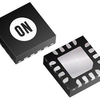
NBSG16MMN ON Semiconductor, NBSG16MMN Datasheet - Page 3

NBSG16MMN
Manufacturer Part Number
NBSG16MMN
Description
IC RCVR/DRVR CML 2.5V/3.3V 16QFN
Manufacturer
ON Semiconductor
Type
Transceiverr
Datasheet
1.NBSG16MMNR2G.pdf
(11 pages)
Specifications of NBSG16MMN
Applications
Instrumentation
Mounting Type
Surface Mount
Package / Case
16-TFQFN Exposed Pad
Logic Family
NBSG
Logic Type
Receiver and Driver Translator Buffer
Supply Voltage (max)
- 3.465 V, 3.465 V
Supply Voltage (min)
- 2.375 V, 2.375 V
Maximum Operating Temperature
+ 85 C
Mounting Style
SMD/SMT
Data Rate
10000 Mbps
Minimum Operating Temperature
- 40 C
Number Of Lines (input / Output)
/ /
Supply Current
51 mA
Lead Free Status / RoHS Status
Contains lead / RoHS non-compliant
Other names
NBSG16MMNOS
Available stocks
Company
Part Number
Manufacturer
Quantity
Price
Company:
Part Number:
NBSG16MMNG
Manufacturer:
ON Semiconductor
Quantity:
135
Part Number:
NBSG16MMNG
Manufacturer:
ON/安森美
Quantity:
20 000
VTD
VTD
V
BB
D
D
50 W
50 W
Figure 2. Logic Diagram
Table 2. Interfacing Options
Table 3. ATTRIBUTES
4. For additional Moisture Sensitivity information, refer to Application Note AND8003/D.
ESD Protection
Moisture Sensitivity, Indefinite Time Out of Drypack (Note 4)
Flammability Rating
Transistor Count
Meets or exceeds JEDEC Spec EIA/JESD78 IC Latchup Test
INTERFACING OPTIONS
V
V
RSECL, PECL, NECL
EE
CC
LVTTL, LVCMOS
AC−COUPLED
LVDS
CML
Characteristics
50 W
http://onsemi.com
Oxygen Index: 28 to 34
Charged Device Model
50 W
Human Body Model
Machine Model
3
Q
Q
Nominal voltage 1.5 V for LVTTL and V
An external voltage should be applied to the
Bias VTD and VTD Inputs within (V
QFN−16
unused complementary differential input.
Standard ECL Termination Techniques
Connect VTD and VTD together
Connect VTD and VTD to V
50 W
Figure 3. CML Output Structure
Common Mode Range
CONNECTIONS
LVCMOS inputs.
Pb Pkg
Level 1
Value
UL 94 V−0 @ 0.125 in
> 100 V
> 1 kV
> 4 kV
V
V
145
CC
EE
Pb−Free Pkg
16 mA
Level 1
CC
IHCMR
CC
/2 for
50 W
)
Q
Q


