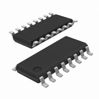
SI8405AB-B-IS1 Silicon Laboratories Inc, SI8405AB-B-IS1 Datasheet - Page 19

SI8405AB-B-IS1
Manufacturer Part Number
SI8405AB-B-IS1
Description
IC ISOLATOR BIDIR I2C 16-SOIC
Manufacturer
Silicon Laboratories Inc
Datasheet
1.SI8401AA-B-ISR.pdf
(34 pages)
Specifications of SI8405AB-B-IS1
Number Of Channels
6
Package / Case
16-SOIC (3.9mm Width)
Inputs - Side 1/side 2
3/3
Isolation Rating
2500Vrms
Voltage - Supply
3 V ~ 5.5 V
Data Rate
10Mbps
Output Type
Open Drain
Operating Temperature
-40°C ~ 125°C
Mounting Style
SMD/SMT
Propagation Delay Time
20 ns
Supply Voltage (max)
5.5 V
Supply Voltage (min)
3 V
Supply Current
6.2 mA
Maximum Operating Temperature
+ 125 C
Minimum Operating Temperature
- 40 C
Lead Free Status / RoHS Status
Lead free / RoHS Compliant
Propagation Delay
-
Lead Free Status / Rohs Status
Lead free / RoHS Compliant
Available stocks
Company
Part Number
Manufacturer
Quantity
Price
Part Number:
SI8405AB-B-IS1
Manufacturer:
SILICON LABS/èٹ¯ç§‘
Quantity:
20 000
Part Number:
SI8405AB-B-IS1R
Manufacturer:
SILICON LABS/èٹ¯ç§‘
Quantity:
20 000
5.3. I
Table 13 lists the design constraints.
5.4. I
The first step in applying an I
Ideally, it should be the side which:
1. Is compatible with the range of bus pull up specified by the manufacturer. For example, the Si8400/01/02/05
2. Has the highest input low level for devices on the bus. Some devices may specify an input low of 0.9 V and
3. Have devices on the bus that can pull down below the isolator input low level. For example, the Si840x input
4. Has the lowest noise. Due to the special logic levels, noise margins can be as low as 50 mV.
The Si840x isolators are not compatible with devices that have a logic low of 0.8 V. For this situation, a discrete
circuit can be used. See “AN352: Low-Cost, High-Speed I
information.
Design Constraint
To prevent the latch condition, the
isolator output low level must be
greater than the isolator input low
level.
The bus output low must be less
than the isolator input low logic
level.
The isolator output low must be
less than the bus input low.
isolators are normally used with a pull up of 0.5 mA to 3 mA.
other devices might require an input low of 0.3 x Vdd. Assuming a 3.3 V minimum power supply, the side with
an input low of 0.3 x Vdd is the better side because this side has an input low level of 1.0 V.
level is 0.45 V. As most CMOS devices can pull to within 0.4 V of GND this is generally not an issue.
2
2
C Isolator Design Constraints
C Isolator Design Considerations
2
C isolator is to choose which side of the bus will be connected to the isolator A side.
Bus V
∆VSDA1, ∆VSCL1 = 50 mV minimum
Isolator V
Table 13. Design Constraints
(0.5 mA pullup, –10 to 125 °C)
Isolator V
Input/Output Logic Low Level
Bus V
IL
Isolator V
Isolator V
0.3 x V
Data Sheet Values
OL
OL
V
Difference
IL
DD
DD
= 0.4 V maximum
= 0.825 V maximum,
= 0.45 V minimum
OL
Rev. 1.3
IL
= 1.0 V minimum for
= 3.3 V
0.6 V typical
0.8 V typical
2
C Isolation with Digital Isolators” for additional
This is normally guaranteed by the
isolator data sheet. However, if the
pull up strength is too weak, the out-
put low voltage will fall and can get
too close to the input low logic level.
These track over temperature.
If the pull up strength is too large,
the devices on the bus might not pull
the voltage below the input low
range. These have opposite temper-
ature coefficients. Worst case is hot
temperature.
If the pull up strength is too large,
the isolator might not pull below the
bus input low voltage.
Si8400/01/05 Vol: –1.8 mV/C
CMOS buffer: –0.6 mV/C
This provides some temperature
tracking, but worst case is cold tem-
perature.
Effect of Bus Pull-up Strength
and Temperature
Si840x
19


