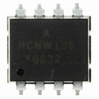
HCNW139-300E Avago Technologies US Inc., HCNW139-300E Datasheet - Page 9

HCNW139-300E
Manufacturer Part Number
HCNW139-300E
Description
OPTOCOUPLER DARL-OUT GW 8-SMD W
Manufacturer
Avago Technologies US Inc.
Specifications of HCNW139-300E
Input Type
DC
Package / Case
8-SMD (400 mil) Gull Wing
Voltage - Isolation
3750Vrms
Number Of Channels
1, Unidirectional
Current - Output / Channel
60mA
Data Rate
100KBd
Propagation Delay High - Low @ If
5µs @ 500µA
Current - Dc Forward (if)
25mA
Output Type
Open Collector
Mounting Type
Surface Mount, Gull Wing
Isolation Voltage
5000 Vrms
Maximum Continuous Output Current
60 mA
Maximum Forward Diode Current
20 mA
Minimum Forward Diode Voltage
1.25 V
Output Device
Darlington With Base
Configuration
1 Channel
Current Transfer Ratio
4500 %(Typ)
Maximum Baud Rate
100 KBps
Maximum Forward Diode Voltage
1.85 V
Maximum Reverse Diode Voltage
3 V
Maximum Input Diode Current
20 mA
Maximum Power Dissipation
135 mW
Maximum Operating Temperature
+ 70 C
Minimum Operating Temperature
0 C
No. Of Channels
1
Optocoupler Output Type
Photodarlington
Input Current
12mA
Output Voltage
18V
Opto Case Style
SMD
No. Of Pins
8
Ctr Min
1500%
Forward Voltage
1.4V
Rohs Compliant
Yes
Data Rate Max
100Kbps
Lead Free Status / RoHS Status
Lead free / RoHS Compliant
Lead Free Status / RoHS Status
Lead free / RoHS Compliant, Lead free / RoHS Compliant
Other names
516-1613-5
Available stocks
Company
Part Number
Manufacturer
Quantity
Price
Company:
Part Number:
HCNW139-300E
Manufacturer:
AVAGO
Quantity:
4 100
Part Number:
HCNW139-300E
Manufacturer:
AVAGO/安华高
Quantity:
20 000
Absolute Maximum Ratings*
*JEDEC Registered Data for 6N139 and 6N138.
**0 C to 70 C on JEDEC Registration.
Recommended Operating Conditions
Storage Temperature
Operating Temperature**
Average Forward Input Current
Peak Forward Input Current
Peak Transient Input Current
Reverse Input Voltage
Input Power Dissipation
Output Current (Pin 6)
Emitter Base Reverse Voltage (Pin 5-7)
Supply Voltage and Output Voltage
(6N139, HCPL-0701, HCNW139)
Supply Voltage and Output Voltage
(6N138, HCPL-0700, HCNW138)
Output Power Dissipation
Total Power Dissipation
Lead Solder Temperature (for Through Hole Devices)
Reflow Temperature Profile
(for SOIC-8 and Option #300)
Power Supply Voltage
Forward Input Current (ON)
Forward Input Voltage (OFF)
Operating Temperature
(50% Duty Cycle, 1 ms Pulse Width)
(<1 s Pulse Width, 300 pps)
Parameter
Parameter
(No Derating Required up to 85 C)
HCNW139/138
HCNW139/138
Symbol
V
I
F(OFF)
F(ON)
V
T
CC
A
260 C for 10 sec., 1.6 mm below seating plane
Symbol
I
I
F(TRAN)
F(AVG)
I
V
V
V
See Package Outline Drawings section
P
T
FPK
V
P
260 C for 10 sec., up to seating plane
T
P
I
EB
CC
CC
O
A
R
O
T
S
I
Min.
4.5
0.5
0
0
9
Min.
-0.5
-0.5
-55
-40
Max.
12.0
0.8
18
70
Max.
125
100
135
1.0
0.5
85
20
40
35
60
18
5
3
7
Units
mA
V
V
Units
C
mW
mW
mW
mA
mA
mA
A
V
V
V
V
V
C
C


