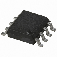
ACSL-6210-00RE Avago Technologies US Inc., ACSL-6210-00RE Datasheet - Page 9

ACSL-6210-00RE
Manufacturer Part Number
ACSL-6210-00RE
Description
OPTOCOUPLER DUAL BI 15MBD 8-SOIC
Manufacturer
Avago Technologies US Inc.
Datasheet
1.ACSL-6210-00RE.pdf
(19 pages)
Specifications of ACSL-6210-00RE
Package / Case
8-SOIC (0.154", 3.90mm Width)
Voltage - Isolation
2500Vrms
Number Of Channels
2, Bi-Directional
Current - Output / Channel
50mA
Data Rate
15MBd
Propagation Delay High - Low @ If
44ns @ 8mA
Current - Dc Forward (if)
15mA
Input Type
DC
Output Type
Open Collector
Mounting Type
Surface Mount
Isolation Voltage
2500 Vrms
Maximum Continuous Output Current
50 mA
Maximum Fall Time
0.012 us
Maximum Forward Diode Current
15 mA
Minimum Forward Diode Voltage
1.25 V
Output Device
Logic Gate Photo IC
Configuration
2 Channel
Maximum Baud Rate
15 MBd(Typ)
Maximum Forward Diode Voltage
1.8 V
Maximum Reverse Diode Voltage
5 V
Maximum Power Dissipation
60 mW
Maximum Operating Temperature
+ 100 C
Minimum Operating Temperature
- 40 C
No. Of Channels
2
Optocoupler Output Type
Logic Gate
Input Current
15mA
Output Voltage
7V
Opto Case Style
SOIC
No. Of Pins
8
Channel Type
Bi-directional
Rohs Compliant
Yes
Lead Free Status / RoHS Status
Lead free / RoHS Compliant
Lead Free Status / RoHS Status
Lead free / RoHS Compliant, Lead free / RoHS Compliant
Other names
516-1602-5
Available stocks
Company
Part Number
Manufacturer
Quantity
Price
Part Number:
ACSL-6210-00RE
Manufacturer:
AVAGO/安华高
Quantity:
20 000
Absolute Maximum Ratings
Parameter
Storage Temperature
Operating Temperature
Supply Voltage (1 Minute Maximum)
Reverse Input Voltage (Per Channel)
Output Voltage (Per Channel)
Average Forward Input Current
Output Current (Per Channel)
Input Power Dissipation
Output Power Dissipation
Recommended Operating Conditions
Parameter
Operating Temperature
Input Current, Low Level
Input Current, High Level
Supply Voltage
Fan Out (at R
Output Pull-up Resistor
Notes:
1. Peaking circuits may produce transient input currents up to 50 mA, 50 ns max. pulse width, provided average current does not exceed its max.
2. Derate total package power dissipation, PT linearly above +95°C free-air temperature at a rate of 1.57mW/°C for the SO8 package mounted on
3. The off condition can be guaranteed by ensuring that V
4. The initial switching threshold is 7 mA or less. It is recommended that minimum 8 mA be used for best performance and to permit guardband
9
values.
low conductivity board per JESD 51-3. Derate total package power dissipation, PT linearly above +80°C free-air temperature at a rate of 1.59
mW/°C for the SO16 package mounted on low conductivity board per JESD 51-3. PT= number of channels multiplied by (PI+PO).
for LED degradation.
100
90
80
70
60
50
40
30
20
10
0
0
20
L
= 1kΩ)
T
so-16 package
so-8 package
A
- Ambient Temperature -
40
60
[2]
[3]
[4]
[2]
(Per Channel)
(Per Channel)
80
[1]
o
C
(Per Channel)
100
120
FL
Symbol
T
T
V
V
V
I
I
P
P
Symbol
T
I
I
V
N
R
F
O
FL
FH
≤ 0.8V.
s
A
A
DD1
R
O
I
O
DD1
L
, V
, V
DD2
DD2
Min.
-55
-40
Min.
-40
0
7
3.0
330
Max.
125
100
7
5
7
15
50
27
65
Max.
100
250
15
5.5
5
4k
Units
°C
°C
V
V
V
mA
mA
mW
mW
Units
°C
μA
mA
V
TTL Loads
Ω


