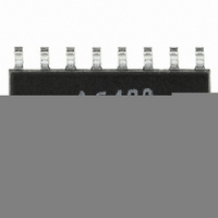
ACSL-6420-00TE Avago Technologies US Inc., ACSL-6420-00TE Datasheet - Page 11

ACSL-6420-00TE
Manufacturer Part Number
ACSL-6420-00TE
Description
OPTOCOUPLER QUAD BIDIR 16-SOIC
Manufacturer
Avago Technologies US Inc.
Datasheet
1.ACSL-6210-00RE.pdf
(19 pages)
Specifications of ACSL-6420-00TE
Voltage - Isolation
2500Vrms
Number Of Channels
4, Unidirectional
Current - Output / Channel
50mA
Data Rate
15MBd
Propagation Delay High - Low @ If
44ns @ 8mA
Current - Dc Forward (if)
15mA
Input Type
DC
Output Type
Open Collector
Mounting Type
Surface Mount
Package / Case
16-SOIC (0.154", 3.90mm Width)
No. Of Channels
4
Optocoupler Output Type
Logic Gate
Input Current
15mA
Output Voltage
7V
Opto Case Style
SOIC
No. Of Pins
16
Propagation Delay Low-high
100ns
Isolation Voltage
2.5kV
Channel Type
Bi-directional
Rohs Compliant
Yes
Lead Free Status / RoHS Status
Lead free / RoHS Compliant
Other names
516-1733-5
ACSL-6420-00TE
ACSL-6420-00TE
Electrical Specifications
Over recommended operating range (4.5V ≤ V
All typical specifications are at T
Parameter
Input Threshold Current
High Level Output Current
Low Level Output Voltage
High Level Supply Current
(per channel)
Low Level Supply Current
(per channel)
Input Forward Voltage
Input Reverse Breakdown Voltage
Input Diode Temperature Coefficient
Input Capacitance
Switching Specifications
Over recommended operating range (4.5V ≤ V
specified. All typical specifications are at T
Parameter
Maximum Data Rate
Pulse Width
Propagation Delay Time
to Logic High Output Level
Propagation Delay Time
to Logic Low Output Level
Pulse Width Distortion |t
Propagation Delay Skew
Output Rise Time (10 – 90%)
Output Fall Time (10 – 90%)
Logic High Common Mode
Transient Immunity
Logic Low Common Mode
Transient Immunity
Notes:
6. t
7. t
8. CM
11
5. t
tions.
voltage slew rate that can be sustained while maintaining V
common mode voltage edges.
PLH
PHL
PSK
is equal to the worst case difference in t
H
is measured from the 4.0 mA level on the falling edge of the input pulse to the 1.5V level on the rising edge of the output pulse.
is measured from the 4.0 mA level on the rising edge of the input pulse to the 1.5V level on the falling edge of the output pulse.
is the maximum common mode voltage slew rate that can be sustained while maintaining V
[8]
[8]
PHL
[7]
[6]
[5]
– t
PLH
A
|
= +25°C, V
PHL
Symbol
I
I
V
I
I
V
BV
∆V
C
Symbol
t
t
t
|PWD|
t
t
t
|CM
|CM
TH
OH
DDH
DDL
PW
PLH
PHL
PSK
R
F
OL
F
IN
A
=+25°C, V
and/or t
DD1
R
F
/ ∆T
H
L
|
|
= V
DD1
DD1
A
DD2
≤ 5.5V, 4.5V ≤ V
PLH
≤ 5.5V, 4.5V ≤ V
= +5.0V.
that will be seen between units at any given temperature and specified test condi-
DD1
Min.
1.25
5.0
Min.
10
100
10
10
O
= V
< 0.8V. The common mode voltage slew rates apply to both rising and falling
DD2
= +5.0V.
DD2
Typ.
2.7
3.8
0.36
4.3
5.8
1.52
-1.8
80
Typ.
15
46
43
5
30
12
DD2
≤ 5.5V, T
≤ 5.5V, I
Max.
7.0
100.0
0.6
7.5
10.5
1.8
Max.
100
100
35
40
A
= -40°C to +100°C) unless otherwise specified.
F
= 8.0 mA, T
Units
MBd
ns
ns
ns
ns
ns
ns
ns
kV/μs
kV/μs
Units
mA
μA
V
mA
mA
V
V
mV/°C
pF
O
> 2.0V. CM
A
= -40°C to +100°C) unless otherwise
Test Conditions
I
I
I
I
I
I
I
I
f = 1 MHz, V
Test Conditions
R
R
R
R
R
R
R
R
V
V
T
V
V
T
OL(Sinking)
F
OL(Sinking)
F
F
F
R
F
A
A
L
L
L
L
L
L
L
L
cm
O
cm
O
= 250 μA, V
= 0 mA
= 10 mA
= 10 mA, T
= 10 μA
= 10 mA
L
= 25°C
= 25°C
= 350Ω, C
= 350Ω, C
= 350Ω, C
= 350Ω, C
= 350Ω, C
= 350Ω, C
= 350Ω, C
= 350Ω, C
= 2.0V, R
= 0.8V, R
= 1000V, I
= 1000V, I
is the maximum common mode
=13 mA, V
=13 mA, I
L
L
F
=350Ω,
= 350Ω,
A
L
L
L
L
L
L
L
L
O
= 0V
F
F
= 25°C
=15 pF
=15 pF
=15 pF
=15 pF
=15 pF
=15 pF
=15 pF
=15 pF
=0 mA,
= 8 mA,
= 5.5V
F
=7 mA
O
= 0.6V


