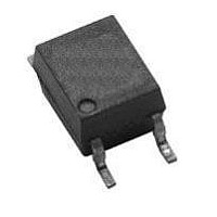
HCPL-M456-500E Avago Technologies US Inc., HCPL-M456-500E Datasheet - Page 6

HCPL-M456-500E
Manufacturer Part Number
HCPL-M456-500E
Description
OPTOCOUPLER IPM 1MBD SO-5
Manufacturer
Avago Technologies US Inc.
Datasheet
1.HCPL-M456500.pdf
(13 pages)
Specifications of HCPL-M456-500E
Voltage - Isolation
3750Vrms
Number Of Channels
1, Unidirectional
Current - Output / Channel
15mA
Propagation Delay High - Low @ If
200ns @ 10mA
Current - Dc Forward (if)
25mA
Input Type
DC
Output Type
Open Collector
Mounting Type
Surface Mount
Package / Case
5-SOP
No. Of Channels
1
Optocoupler Output Type
Gate Drive
Input Current
20mA
Output Voltage
30V
Opto Case Style
SOIC
No. Of Pins
5
Ctr Max
90%
Isolation Voltage
3.75kV
Lead Free Status / RoHS Status
Lead free / RoHS Compliant
Available stocks
Company
Part Number
Manufacturer
Quantity
Price
Company:
Part Number:
HCPL-M456-500E
Manufacturer:
AVAGO
Quantity:
26 000
Part Number:
HCPL-M456-500E
Manufacturer:
AVAGO/安华高
Quantity:
20 000
Part Number:
HCPL-M456-500E/HCPLM456-500E
Manufacturer:
AVAGO/安华高
Quantity:
20 000
Switching Specifications (R
Over recommended operating conditions unless otherwise specified:
T
*All typical values at 5°C, V
Notes:
10. The difference between t
11. Common mode transient immunity in a Logic High level is the maximum tolerable dV
1. Common mode transient immunity in a Logic Low level is the maximum tolerable dV
13. Pulse Width Distortion (PWD) is defined as |t
6
A
1. Derate linearly above 90°C free-air temperature at a rate of 0.8 mA/°C.
. Derate linearly above 90°C free-air temperature at a rate of 1.6 mA/°C.
3. Derate linearly above 90°C free-air temperature at a rate of 3.0 mW/°C.
4. Derate linearly above 90°C free-air temperature at a rate of 4. mW/°C.
5. CURRENT TRANSFER RATIO in percent is defined as the ratio of output collector current (I
6. Device considered a two-terminal device: Pins 1 and 3 shorted together and Pins 4, 5 and 6 shorted together.
7. In accordance with UL1577, each optocoupler is proof tested by applying an insulation test voltage ≥ 4500 V
8. Pulse: f = 0 kHz, Duty Cycle = 10%.
9. Use of a 0.1 µF bypass capacitor connected between pins 4 and 6 can improve performance by filtering power supply line noise.
Propagation Delay
Time to Low
Output Level
Propagation Delay
Time to High
Output Level
Pulse Width
Distortion
Propagation Delay
Difference Between
Any Parts
Output High Level
Common Mode
Transient Immunity
Output Low Level
Common Mode
Transient Immunity
= -40°C to +100°C, V
tion current limit, I
fications section.)
the output will remain in a Logic High state (i.e., V
output will remain in a Logic Low state (i.e., V
Parameter
I-O
≤ 5 µA).
CC
CC
PLH
= 15 V.
= +4.5 V to 30 V, I
t
and t
PLH
Symbol
|CM
|CM
PWD
L
t
t
= 20 kΩ)
PHL
PLH
-t
PHL
H
PHL
L
|
|
between any two parts under the same test condition. (See IPM Dead Time and Propagation Delay Speci-
-150
30
70
Min.
15
15
PHL
O
< 1.0 V).
- t
F(on)
PLH
Typ.*
O
00
00
00
100
400
130
30
30
> 3.0 V).
| for any given device.
= 10 mA to 0 mA, V
Max.
450
450
400
550
kV/µs
kV/µs
Units
ns
ns
ns
ns
ns
F(off )
C
I
V
I
V
C
C
C
C
F
F
O
O
L
L
L
L
L
= 0 mA,
= 10 mA,
= 100 pF
> 3.0 V
< 1.0 V
= 100 pF
= 100 pF
= 10 pF
= 10 pF
= -5 V to 0.8 V
CM
CM
/dt of the common mode pulse, V
/dt of the common mode pulse, V
O
Test Conditions
) to the forward LED input current (I
I
V
V
V
V
V
C
V
T
F(on)
CC
CC
CM
F(off )
THLH
THHL
L
A
= 100 pF,
= 5°C
= 15.0 V,
= 15.0 V,
= 1500 V
= 10 mA,
= 0.8 V,
= .0 V,
= 1.5 V
RMS
for 1 second (leakage detec-
P-P
,
CM
CM
, to assure that the
, to assure that
8-1
Fig.
F
6,
) times 100.
7
Note
8, 9
13
10
11
1


