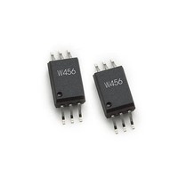
ACPL-W456-520E Avago Technologies US Inc., ACPL-W456-520E Datasheet - Page 10

ACPL-W456-520E
Manufacturer Part Number
ACPL-W456-520E
Description
OPTOCOUPLER IPM GATE DRV 6-SOIC
Manufacturer
Avago Technologies US Inc.
Specifications of ACPL-W456-520E
Output Type
Open Collector
Package / Case
SO-6
Voltage - Isolation
5000Vrms
Number Of Channels
1, Unidirectional
Current - Output / Channel
15mA
Propagation Delay High - Low @ If
200ns @ 10mA
Current - Dc Forward (if)
25mA
Input Type
DC
Mounting Type
Surface Mount
Logic Gate Type
Power Module and Gate Drive Interface Optocouplers
Configuration
1 Channel
Isolation Voltage
3750 Vrms
Current Transfer Ratio
44 %
Maximum Propagation Delay Time
550 ns
Maximum Forward Diode Voltage
0.8 V
Minimum Forward Diode Voltage
- 5 V
Maximum Forward Diode Current
20 mA
Maximum Continuous Output Current
15 mA
Maximum Power Dissipation
145 mW
Maximum Operating Temperature
+ 100 C
Minimum Operating Temperature
- 40 C
Lead Free Status / RoHS Status
Lead free / RoHS Compliant
Figure 16. AC Equivalent Circuit for Figure 15 during Common Mode Tran-
sients.
Figure 17. AC Equivalent Circuit for Figure 12 during Common Mode Tran-
sients.
CMR With The LED Off (CMR
A high CMR LED drive circuit must keep the LED off (V
≤ V
during a +dV
flowing through C
bination of the LED and series resistor. As long as the
voltage developed across the resistor is less than V
the LED will remain off and no common mode failure
will occur. Even if the LED momentarily turns on, the
100 pF capacitor from pins 5-4 will keep the output from
dipping below the threshold. The recommended LED
drive circuit (Figure 12) provides about 10 V of margin
between the lowest optocoupler output voltage and a
3 V IPM threshold during a 15kV/μs transient with V
= 1500 V. Additional margin can be obtained by adding
a diode in parallel with the resistor, as shown by the
dashed line connection in Figure 17, to clamp the voltage
across the LED below V
10
F(OFF)
+ V
I
300 Ω
TOTAL
300 Ω
* THE ARROWS INDICATE THE DIRECTION OF CURRENT
FLOW FOR + dV
** OPTIONAL CLAMPING DIODE FOR IMPROVED CMH
PERFORMANCE. V
R
** -
*
-
) during common mode transients. For example,
1
2
3
* THE ARROWS INDICATE THE DIRECTION
OF CURRENT FLOW DURING + dV
1
2
3
I
CLEDP
I
C
F
I
CM
LEDN
CLEDN
C
LEDP
CM
/dt transient in Figure 17, the current
* C
R
/dt TRANSIENTS.
< V
LEDN
LEDN
F (OFF)
SHIELD
SHIELD
I
CLED01
V
SHIELD
F(OFF)
DURING + dV
CM
V
is supplied by the parallel com-
CM
C
H
LED01
.
C
)
LED01
CM
CM
/dt
/dt
6
5
4
6
5
4
V
OUT
V
OUT
20 kΩ
100 pF
20 kΩ
100 pF
pF
F(OFF)
CM
F
Since the open collector drive circuit, shown in Figure 18,
cannot keep the LED off during a +dV
not desirable for applications requiring ultra high CMR
performance. Figure 19 is the AC equivalent circuit for
Figure 18 during common mode transients. Essentially
all the current flowing through C
transient must be supplied by the LED. CMR
occur at dv/dt rates where the current through the LED
and C
ternative drive circuit which does achieve ultra high CMR
performance by shunting the LED in the off state.
Figure 18. Not Recommended Open Collector LED Drive Circuit.
Figure 19. AC Equivalent Circuit for Figure 18 during Common Mode Tran-
sients.
Figure 20. Recommended LED Drive Circuit for Ultra High CMR.
+5 V
Q1
+5 V
Q1
Q1
LEDN
300 Ω
* THE ARROWS INDICATE THE DIRECTION OF CURRENT
FLOW FOR + dV
exceeds the input threshold. Figure 20 is an al-
1
2
3
1
2
3
1
2
3
I
CLEDN
C
C
LEDP
LEDP
* C
CM
LEDN
/dt TRANSIENTS.
SHIELD
SHIELD
SHIELD
V
CM
C
LED01
LEDN
6
5
4
CM
6
5
4
6
5
4
during a +dV
/dt transient, it is
V
OUT
H
failures can
20 kΩ
100 pF
CM
/dt
H


