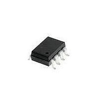
HCPL-3150#500 Avago Technologies US Inc., HCPL-3150#500 Datasheet

HCPL-3150#500
Specifications of HCPL-3150#500
Available stocks
Related parts for HCPL-3150#500
HCPL-3150#500 Summary of contents
Page 1
... The voltage and current supplied by this opto- coupler makes it ideally suited for directly driving IGBTs with ratings up to 1200 V/50 A. For IGBTs with higher rat- ings, the HCPL-3150/315J can be used to drive a discrete power stage which drives the IGBT gate. Applications ...
Page 2
... Current CMR 15 kV/μs (minimum) UVLO Yes Fault Status Ordering Information HCPL-3150 is UL Recognized with 3750 Vrms for 1 minute per UL1577. HCPL-315J is UL Recognized with 5000 Vrms for 1 minute per UL1577. Option Part RoHS Non RoHS Number Compliant Compliant -000E ...
Page 3
Package Outline Drawings Standard DIP Package 9.40 (0.370) 9.90 (0.390 3150 Z YYWW PIN ONE 1.78 (0.070) MAX. 1.19 (0.047) MAX. 3.56 ± 0.13 (0.140 ± 0.005) PIN ONE 2.92 (0.115) ...
Page 4
... Lead Surface Mount 10.36 ± 0.20 HCPL-315J (0.408 ± 0.008 VIEW FROM PIN 16 9° VIEW FROM PIN 1 (0.018) 0.457 (0.406 ± 0.007) 10.31 ± 0.18 4 LAND PATTERN RECOMMENDATION (0.295 ± 0.004) 7.49 ± 0. (0.025) 0.64 (0.004 – 0.011) 0.10 – 0.30 (0.345 ± ...
Page 5
... Recommended Pb-Free IR Profile Recommended reflow condition as per JEDEC Standard, J-STD-020 (latest revision). Non-Halide Flux should be used. Regulatory Information The HCPL-3150 and HCPL-315J have been approved by the following organizations: UL Recognized under UL 1577, Component Recognition Program, File E55361. CSA Approved under CSA Component Acceptance Notice #5, File CA 88324 ...
Page 6
... Output Power Dissipation Total Power Dissipation Lead Solder Temperature Solder Reflow Temperature Profile Recommended Operating Conditions Parameter Symbol Power Supply Voltage (V Input Current (ON) Input Voltage (OFF) Operating Temperature 6 HCPL-3150 HCPL-315J 7.1 8.3 7.4 8.3 0.08 ≥0.5 ≥175 ≥175 IIIa IIIa Symbol Min. T ...
Page 7
... 11.0 12.3 13.5 V 9.5 10.7 12.0 1 unless otherwise noted -3 F(OFF) CC Test Conditions Fig 2 -100 100 Output Open Output Open -3 HCPL-3150 mA, 9, 15, O HCPL-315J V > HCPL-3150 HCPL-315J = HCPL-3150 μA R HCPL-315J μ MHz > 22 Note ...
Page 8
Switching Specifications (AC) Over recommended operating conditions ( Ground, each channel) unless otherwise specified. EE Parameter Symbol Propagation Delay t PLH Time to High Output Level Propagation Delay t PHL Time to Low Output Level Pulse Width PWD ...
Page 9
... Maximum pulse width = 1 ms, maximum duty cycle = 20 accordance with UL1577, each HCPL-3150 optocoupler is proof tested by applying an insulation test voltage ≥4500 Vrms (≥ 6000 Vrms for the HCPL-315J) for 1 second. This test is performed before the 100% production test for partial discharge (method b) shown in the IEC/EN/ DIN EN 60747-5-2 Insulation Characteristics Table, if applicable ...
Page 10
-100 mA OUT -40 - 100 T – TEMPERATURE ...
Page 11
PLH ° PHL Ω 400 DUTY CYCLE = 50 kHz 300 200 100 ...
Page 12
Figure 17. I Test Circuit Figure 19. V Test Circuit ...
Page 13
... OL 3150/315J realizes this very low V transistor with 4 Ω (typical) on resistance in its pull down circuit. When the HCPL-3150/315J is in the low state, the IGBT gate is shorted to the emitter Ω. Minimiz- ing Rg and the lead inductance from the HCPL-3150/315J to the IGBT gate and emitter (possibly by mounting the ...
Page 14
... HCPL-315J FLOATING SUPPLY 0.1 μF + – 0.1 μF + – Step 2: Check the HCPL-3150/315J Power Dissipation and Increase Rg if Necessary. The HCPL-3150/315J total power dissipa tion Peak Specifica tion. The ( equal to the sum of the emitter power (P T output power ( Duty Cycle O(BIAS) ...
Page 15
... CONTROL INPUT 2 74XX OPEN COLLECTOR 3 GND 270 Ω CONTROL 7 INPUT 74XX OPEN 8 COLLECTOR GND 1 Figure 26b. HCPL-315J Typical Application Circuit with Negative IGBT Gate Drive Parameter Description I LED Current F V LED On Voltage F Duty Cycle Maximum LED Duty Cycle 0.1 μF + – ...
Page 16
... For Qg = 500 nC, from Figure 27, a value of E gives Ω. Thermal Model (HCPL-3150) The steady state thermal model for the HCPL-3150 is shown in Figure 28a. The thermal resistance values given in this model can be used to calculate the tempera tures at each node for a given operating condition. As shown ...
Page 17
... T through Thermal Coefficient Data (units in °C/W) Part Number HCPL-315J 198 Note: Maximum junction temperature for above part: 125°C. 17 DETECTOR 1 θ 7 Figure 28b. Thermal Impedance Model for HCPL-315J θ 1 LED 1 LED 2 θ θ ...
Page 18
... HCPL-3150/315J V the optocoupler output will go into the low state with a typical delay, UVLO Turn Off Delay, of 0.6 μs. When the HCPL-3150/315J output is in the low state and the supply voltage rises above the HCPL-3150/315J achieve (11.0 < V < ...
Page 19
... Figure 35. The maxi- mum dead time for the HCPL-3150/315J is 700 ns (= 350 ns - (-350 ns)) over an operating temperature range of -40°C to 100°C. Note that the propagation delays used to calculate PDD ...
Page 20
V C LEDP LEDN I LEDN 4 SHIELD Figure 32. Not Recommended Open Collector Drive Circuit. I LED1 V OUT1 OFF V OUT2 I LED2 t PHL MAX t PLH MIN ...
Page 21
... T – CASE TEMPERATURE – °C S Figure 37b. HCPL-315J: Thermal Derating Curve, Dependence of Safety Limiting Value with Case Temperature per IEC/EN/DIN EN 60747-5-2. For product information and a complete list of distributors, please go to our website: Avago, Avago Technologies, and the A logo are trademarks of Avago Technologies in the United States and other countries. ...


