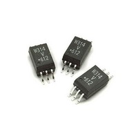
ACPL-W314-060E Avago Technologies US Inc., ACPL-W314-060E Datasheet - Page 11

ACPL-W314-060E
Manufacturer Part Number
ACPL-W314-060E
Description
OPTOCOUPLER IGBT 0.4A VDE 6-SOIC
Manufacturer
Avago Technologies US Inc.
Specifications of ACPL-W314-060E
Output Type
Push-Pull, Totem-Pole
Package / Case
6-SOP
Voltage - Isolation
3750Vrms
Number Of Channels
1, Unidirectional
Current - Output / Channel
600mA
Propagation Delay High - Low @ If
300ns @ 7mA
Current - Dc Forward (if)
25mA
Input Type
DC
Mounting Type
Surface Mount
Fall Time
50 ns
Rise Time
50 ns
Configuration
1 Channel
Isolation Voltage
3750 Vrms
Maximum Propagation Delay Time
700 ns
Maximum Forward Diode Voltage
1.8 V
Minimum Forward Diode Voltage
1.2 V
Maximum Reverse Diode Voltage
5 V
Maximum Forward Diode Current
12 mA
Maximum Power Dissipation
250 mW
Maximum Operating Temperature
+ 100 C
Minimum Operating Temperature
- 40 C
Number Of Elements
1
Forward Voltage
1.8V
Forward Current
25mA
Operating Temp Range
-40C to 100C
Power Dissipation
250mW
Propagation Delay Time
700ns
Pin Count
6
Mounting
Surface Mount
Reverse Breakdown Voltage
5V
Operating Temperature Classification
Industrial
Lead Free Status / RoHS Status
Lead free / RoHS Compliant
Lead Free Status / RoHS Status
Lead free / RoHS Compliant, Lead free / RoHS Compliant
Applications Information
Eliminating Negative IGBT Gate Drive
To keep the IGBT firmly off, the ACPL-P314/W314 has a
very low maximum V
R
to the IGBT gate and emitter (possibly by mounting the
ACPL-P314/W314 on a small PC board directly above the
IGBT) can eliminate the need for negative IGBT gate drive
in many applications as shown in Figure 19. Care should
be taken with such a PC board design to avoid routing
the IGBT collector or emitter traces close to the ACPL-
P314/W314 input as this can result in unwanted coupling
of transient signals into the input of ACPL-P314/W314
and degrade performance. (If the IGBT drain must be
routed near the ACPL-P314/W314 input, then the LED
should be reverse biased when in the off state, to prevent
the transient signals coupled from the IGBT drain from
turning on the ACPL-P314/W314.
Selecting the Gate Resistor (Rg)
Step 1: Calculate R
cation. The IGBT and R
a simple RC circuit with a voltage supplied by the ACPL-
P314/W314.
The V
the peak current of 0.6A. (See Figure 6).
Step 2: Check the ACPL-P314/W314 power dissipation
and increase R
CONTROL
Figure 19. Recommended LED Drive and Application Circuit for ACPL-P314/W314
11
R
g
g
INPUT
and the lead inductance from the ACPL-P314/W314
≥
COLLECTOR
OL
=
=
V
+5 V
C C
I
3 2
2 4
OLPEAK
value of 1 V in the previous equation is the V
74XXX
OPEN
0.6
−
Ω
−
V
5
O L
g
if necessary. The ACPL-P314/W314 total
g
270 Ω
minimum from the I
OL
1
1
2
3
g
specification of 1.0 V. Minimizing
in Figure 19 can be analyzed as
ACPL-P314/W314
OL
peak specifi-
OL
0.1 µF
6
5
4
at
Figure 20. Energy Dissipated in the ACPL-P314/W314 and for Each IGBT Switching
Cycle.
power dissipation (P
power (P
where K
and K
circuit in Figure 19 with I
W, Max Duty Cycle = 80%, Q
T
The value of 3 mA for I
max. I
Since P
alright for the power dissipation.
P
P
P
P
P
AMAX
T
E
O
E
O
+
+
-
-
=
=
=
=
V
=
=
CC
I
P
P
10mA
F
(
(
0.4ì .
I
E
3mA
CC
= 15V
O(BIAS)
CCBIAS
ICC
•
= 85°C:
+
O
V
ICC
R
over entire operating temperature range.
P
E
F
g
for this case is less than P
is a constant of 0.001 mA/(nC*kHz). For the
•
) and the output power (P
O
•
+
+
•
+
20kHz
· Q
DutyCycle
1.8V
P
K
(
Q1
Q2
0.001mA
O(SWITCHIN
ICC
g
•
· f is the increase in I
•
Q
=
0.8
G )
g
128mW
•
T
=
=
) is equal to the sum of the emitter
f
n C
)
I
14mW
CC
C C
•
•
V
F
•
in the previous equation is the
C C
kHz
(worst case) = 10 mA, R
≤
V
C C
+
250mW
g
)
E
+
•
= 100 nC, f = 20 kHz and
S W
E
20kHz
S W
(
R
(
g
(
R
O
P
3-PHASE
Q ;
O(MAX)
CC
).
g
O
+ HVDC
- HVDC
•
Q ;
(
AC
g
MAX
100nC
)
due to switching
•
g
)
)
@85
f
•
, R
f
)
g
°
•
C
= 32 W is
24V
)
g
+
= 32


