HCPL-5531#100 Avago Technologies US Inc., HCPL-5531#100 Datasheet - Page 2
HCPL-5531#100
Manufacturer Part Number
HCPL-5531#100
Description
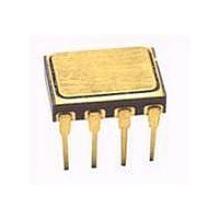
ISOLAT 1.5KVDC 2CH OPEN 8SMD BJ
Manufacturer
Avago Technologies US Inc.
Datasheet
1.HCPL-5500.pdf
(13 pages)
Specifications of HCPL-5531#100
Input Type
DC
Package / Case
8-SMD Butt Joint
Voltage - Isolation
1500VDC
Number Of Channels
2, Unidirectional
Current - Output / Channel
8mA
Data Rate
400kbps
Propagation Delay High - Low @ If
400ns @ 16mA
Current - Dc Forward (if)
20mA
Output Type
Open Collector
Mounting Type
Surface Mount
Output Device
Phototransistor
Configuration
2 Channel
Current Transfer Ratio
20 %
Maximum Baud Rate
400 KBps
Maximum Forward Diode Voltage
1.9 V
Maximum Input Diode Current
20 mA
Maximum Power Dissipation
200 mW
Maximum Operating Temperature
+ 125 C
Minimum Operating Temperature
- 55 C
Lead Free Status / RoHS Status
Contains lead / RoHS non-compliant
Available stocks
Company
Part Number
Manufacturer
Quantity
Price


Each channel contains a GaAsP light emitting diode which
is optically coupled to an integrated photon detector.
Separate connections for the photodiodes and output
transistor collectors improve the speed up to a hundred
times that of a conventional phototransistor optocoupler
by reducing the base-collector capacitance.
These devices are suitable for wide bandwidth analog
applications, as well as for interfacing TTL to LSTTL or
CMOS. Current Transfer Ratio (CTR) is 9% minimum at I
= 16 mA. The 18 V V
to interface any TTL family to CMOS. The availability of
the base lead allows optimized gain/ bandwidth adjust-
ment in analog applications. The shallow depth of the
IC photodiode provides better radiation immunity than
conventional phototransistor couplers.
These products are also available with the transistor base
node not connected to improve common mode noise
immunity and ESD susceptibility. In addition, higher CTR
minimums are available by special request.
Package styles for these parts are 8 and 16 pin DIP through
hole (case outlines P and E respectively), 16 pin DIP flat
pack (case outline F), and leadless ceramic chip carrier
(case outline 2). Devices may be purchased with a variety
of lead bend and plating options, see Selection Guide Table
for details. Standard Microcircuit Drawing (SMD) parts are
available for each package and lead style.
Because the same functional die (emitters and detectors)
are used for each channel of each device listed in this
data sheet, absolute maximum ratings, recommended
operating conditions, electrical specifications, and perfor-
mance characteristics shown in the figures are identical
for all parts. Occasional exceptions exist due to package
variations and limitations and are as noted. Additionally,
the same package assembly processes and materials are
used in all devices. These similarities give justification for
the use of data obtained from one part to represent other
part’s performance for die related reliability and certain
limited radiation test results.
CC
capability will enable the designer
F
Truth Table
(Positive Logic)
Functional Diagram
Multiple Channel Devices Available
On (H)
Off (L)
Input
GND
V
Output
V
CC
V
B
O
H
L
Related parts for HCPL-5531#100
Image
Part Number
Description
Manufacturer
Datasheet
Request
R

Part Number:
Description:
OPTOCOUPLER PHOTOTRANS 4-SMD
Manufacturer:
Avago Technologies US Inc.
Datasheet:

Part Number:
Description:
OPTOCOUPLER TRANS-OUT 1MBD 8-DIP
Manufacturer:
Avago Technologies US Inc.
Datasheet:
Part Number:
Description:
OPTOCOUPLER T-OUT 2CH 1MBD 8-DIP
Manufacturer:
Avago Technologies US Inc.
Datasheet:

Part Number:
Description:
OPTOCOUPLER T-OUT 2CH 1MBD 8SOIC
Manufacturer:
Avago Technologies US Inc.
Datasheet:
Part Number:
Description:
OPTOCOUPLER T-OUT 1MBD 8-DIP
Manufacturer:
Avago Technologies US Inc.
Datasheet:
Part Number:
Description:
OPTOCOUPLER TRANS-OUT 1MBD 8DIP
Manufacturer:
Avago Technologies US Inc.
Datasheet:

Part Number:
Description:
OPTOCOUPLER 1MBD ALGAAS 8-SMD
Manufacturer:
Avago Technologies US Inc.
Datasheet:
Part Number:
Description:
OPTOCOUPLER TRANS-OUT 1MBD 8SOIC
Manufacturer:
Avago Technologies US Inc.
Datasheet:

Part Number:
Description:
OPTOCOUPLER 1CH 2.5MBD 8-DIP
Manufacturer:
Avago Technologies US Inc.
Datasheet:
Part Number:
Description:
OPTOCOUPLR T-OUT 2CH 1MBD 8-DIP
Manufacturer:
Avago Technologies US Inc.
Datasheet:
Part Number:
Description:
OPTOCOUPLER 2CH 1MBS 8-DIP
Manufacturer:
Avago Technologies US Inc.
Datasheet:
Part Number:
Description:
OPTOCOUPLER 2CH CLASS H 8DIP
Manufacturer:
Avago Technologies US Inc.
Datasheet:
Part Number:
Description:
OPTOCOUPLER 1CH 1MBS 8-SOIC
Manufacturer:
Avago Technologies US Inc.
Datasheet:
Part Number:
Description:
OPTOCOUPLER PHOTOTRANS 4-MINIPAK
Manufacturer:
Avago Technologies US Inc.
Datasheet:

Part Number:
Description:
OPTOCOUPLER PHOTOX VDE 4-MINIPAK
Manufacturer:
Avago Technologies US Inc.
Datasheet: