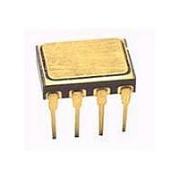
HCPL-5431#100 Avago Technologies US Inc., HCPL-5431#100 Datasheet - Page 9

HCPL-5431#100
Manufacturer Part Number
HCPL-5431#100
Description
ISOLAT 1.5KVDC 2CH TOTEM 8SMD BJ
Manufacturer
Avago Technologies US Inc.
Datasheet
1.HCPL-5400.pdf
(12 pages)
Specifications of HCPL-5431#100
Package / Case
8-SMD Butt Joint
Voltage - Isolation
1500VDC
Number Of Channels
2, Unidirectional
Current - Output / Channel
25mA
Data Rate
40Mbps
Propagation Delay High - Low @ If
33ns @ 10mA
Current - Dc Forward (if)
10mA
Input Type
DC
Output Type
Push-Pull, Totem-Pole
Mounting Type
Surface Mount
Maximum Continuous Output Current
25 mA
Maximum Fall Time
10 ns
Maximum Forward Diode Current
10 mA
Maximum Rise Time
15 ns
Minimum Forward Diode Voltage
1 V
Output Device
Logic Gate Photo IC
Configuration
2 Channel
Maximum Baud Rate
40 MBps
Maximum Forward Diode Voltage
1.85 V
Maximum Reverse Diode Voltage
3 V
Maximum Power Dissipation
200 mW
Maximum Operating Temperature
+ 125 C
Minimum Operating Temperature
- 55 C
Lead Free Status / RoHS Status
Contains lead / RoHS non-compliant
Available stocks
Company
Part Number
Manufacturer
Quantity
Price
INPUT V
MONITORING
NODE
INPUT
MONITORING
NODE
Figure 5. Test circuit for t
9
Figure 6. Typical propagation delay vs.
ambient temperature
Figure 8. Test circuit for t
E
PULSE GEN.
t
I
25 % DUTY
f = 500 kHz
F
r
GENERATOR
C1
15 pF
t
= t
CYCLE
r
Z
= t
PULSE
O
f =
= 50
f =
5 ns
THE PROBE AND JIG CAPACITANCES
ARE REPRESENTED BY C
ALL DIODES ARE 1N4150 OR EQUIVALENT.
5 ns
100
I
F
1
2
3
4
PLH
PHZ
, t
, t
D.U.T.
D.U.T.
PHL
PZH
, t
GND
V
, t
CC
GND
r
V
1
, and t
PLZ
CC
AND C
8
7
6
5
, and t
f
V
V
2 .
CC
CC
PZL
V
O
0.1 µF
0.1 µF
. (single channel product only)
C1
30 pF
MONITORING
30 pF
C2
OUTPUT
NODE
V
2.5 K
O
D
2.5 K
1
5.0 V
S2
5.0 V
S1
1.3 K
D
D
D
2
3
4
1.3 K
Figure 7. Typical propagation delay vs.
input forward current


