TLP350 Toshiba, TLP350 Datasheet - Page 2
TLP350
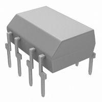
Manufacturer Part Number
TLP350
Description
IC PHOTOCOUPLER IRED 8-DIP
Manufacturer
Toshiba
Specifications of TLP350
Voltage - Isolation
3750Vrms
Number Of Channels
1, Unidirectional
Current - Output / Channel
2.5A
Propagation Delay High - Low @ If
260ns @ 5mA ~ 0mA
Current - Dc Forward (if)
20mA
Input Type
DC
Output Type
Push-Pull, Totem-Pole
Mounting Type
Through Hole
Package / Case
8-DIP (0.300", 7.62mm)
Lead Free Status / RoHS Status
Contains lead / RoHS non-compliant
Available stocks
Company
Part Number
Manufacturer
Quantity
Price

Part Number:
TLP350
Manufacturer:
TOSHIBA/东芝
Quantity:
20 000
Part Number:
TLP350(D4,F)
Manufacturer:
TOSHIBA/东芝
Quantity:
20 000
Company:
Part Number:
TLP350(F)
Manufacturer:
TOSHIBA
Quantity:
250
Part Number:
TLP350(F)
Manufacturer:
TOSHIBA/东芝
Quantity:
20 000
Company:
Part Number:
TLP350(TP1Ј¬F)
Manufacturer:
TOSHIBA
Quantity:
7 500
Part Number:
TLP350(TP1,F)
Manufacturer:
TOSHIBA/东芝
Quantity:
20 000
Company:
Part Number:
TLP3501
Manufacturer:
TOS
Quantity:
5 510
Company:
Part Number:
TLP3501
Manufacturer:
VIKING
Quantity:
5 510
Company:
Part Number:
TLP3502
Manufacturer:
TOSHIBA
Quantity:
6 000
Part Number:
TLP3502
Manufacturer:
TOSHIBA/东芝
Quantity:
20 000


Absolute
Recommended Operating Conditions
Operating frequency
Storage temperature range
Operating temperature range
Lead soldering temperature (10 s)
Isolation voltage (AC, 1 minute, R.H. ≤ 60%)
Note: Using continuously under heavy loads (e.g. the application of high temperature/current/voltage and the
Note 1: Pulse width P
Note 2: Exponential waveform pulse width P
Note 3: Exponential waveform I
Note 4: At 2 mm or more from the lead root.
Note 5: This device is regarded as a two terminal device: pins 1, 2, 3 and 4 are shorted together, as are pins 5, 6, 7
Note 6: A ceramic capacitor(0.1 μF) should be connected from pin 8 to pin 5 to stabilize the operation of the high
Input current, ON
Input voltage, OFF
Supply voltage
Peak output current
Operating temperature
Note: Recommended operating conditions are given as a design guideline to obtain expected performance of the
Note 7: Input signal rise time (fall time) < 0.5 μs.
Note 8: If the rising slope of the supply voltage (VCC) for the detector is steep, stable operation of the internal
Forward current
Forward current derating (Ta ≥ 85°C)
Peak transient forward current
Reverse voltage
Junction temperature
“H” peak output current
“L” peak output current
Supply voltage
Supply voltage Derating
Junction temperature
significant change in temperature, etc.) may cause this product to decrease in the reliability significantly even
if the operating conditions (i.e. operating temperature/current/voltage, etc.) are within the absolute maximum
ratings.
Please design the appropriate reliability upon reviewing the Toshiba Semiconductor Reliability Handbook
(“Handling Precautions”/“Derating Concept and Methods”) and individual reliability data (i.e. reliability test
report and estimated failure rate, etc).
device. Additionally, each item is an independent guideline respectively. In developing designs using this
product, please confirm specified characteristics shown in this document.
Maximum Ratings
and 8.
gain linear amplifier. Failure to provide the bypass may impair the switching property.
The total lead length between capacitor and coupler should not exceed 1 cm.
circuits cannot be guaranteed.
Be sure to set 3.0V/μs or less for a rising slope of the VCC.
Characteristic
Characteristic
W
≤ 1 μs, 300 pps
(Note 7)
OPH
Ta = −40 to 100°C
(Ta = 25°C)
I
≥ -2.0A (≤ 0.3μs), I
OPH
V
Symbol
I
F (OFF)
F (ON)
(Note 2)
V
T
Ta < 95 °C
Ta ≥ 95 °C
CC
opr
/I
OPL
(Note 1)
(Note 3)
(Note 4)
(Note 5)
W
≤ 0.3μs, f ≤ 15kHz
Min
−40
7.5
15
⎯
0
ΔV
2
ΔI
Symbol
OPL
I
CC
I
V
T
BV
F
T
T
OPH
I
OPL
V
Typ.
FP
I
T
T
/ΔTa
CC
stg
opr
sol
f
F
⎯
⎯
⎯
⎯
⎯
R
j
j
/ΔTa
S
≤ 2.0A (≤ 0.3μs)
±2.0
Max
100
0.8
10
30
−55 to 125
−40 to 100
Rating
−0.54
3750
−2.5
125
-1.0
125
260
2.5
20
35
50
1
5
Unit
mA
°C
V
V
A
mA/°C
V /℃
Vrms
Unit
kHz
mA
°C
°C
°C
°C
°C
A
V
A
A
V
2007-10-01
TLP350
Related parts for TLP350
Image
Part Number
Description
Manufacturer
Datasheet
Request
R

Part Number:
Description:
Toshiba Semiconductor [TOSHIBA IGBT Module Silicon N Channel IGBT]
Manufacturer:
TOSHIBA Semiconductor CORPORATION
Datasheet:
Part Number:
Description:
TOSHIBA GTR MODULE SILICON NPN TRIPLE DIFFUSED TYPE
Manufacturer:
TOSHIBA Semiconductor CORPORATION
Datasheet:
Part Number:
Description:
TOSHIBA GTR Module Silicon N Channel IGBT
Manufacturer:
TOSHIBA Semiconductor CORPORATION
Datasheet:
Part Number:
Description:
TOSHIBA Intelligent Power Module Silicon N Channel IGBT
Manufacturer:
TOSHIBA Semiconductor CORPORATION
Datasheet:
Part Number:
Description:
TOSHIBA INTELLIGENT POWER MODULE SILICON N CHANNEL LGBT
Manufacturer:
TOSHIBA Semiconductor CORPORATION
Datasheet:
Part Number:
Description:
TOSHIBA IGBT Module Silicon N Channel IGBT
Manufacturer:
TOSHIBA Semiconductor CORPORATION
Datasheet:
Part Number:
Description:
TOSHIBA GTR MODULE SILICON N−CHANNEL IGBT
Manufacturer:
TOSHIBA Semiconductor CORPORATION
Datasheet:
Part Number:
Description:
TOSHIBA Intelligent Power Module Silicon N Channel IGBT
Manufacturer:
TOSHIBA Semiconductor CORPORATION
Datasheet:
Part Number:
Description:
TOSHIBA GTR Module Silicon N Channel IGBT
Manufacturer:
TOSHIBA Semiconductor CORPORATION
Datasheet:
Part Number:
Description:
TOSHIBA INTELLIGENT POWER MODULE
Manufacturer:
TOSHIBA Semiconductor CORPORATION
Datasheet:
Part Number:
Description:
TOSHIBA Intelligent Power Module Silicon N Channel IGBT
Manufacturer:
TOSHIBA Semiconductor CORPORATION
Datasheet:
Part Number:
Description:
TOSHIBA Intelligent Power Module Silicon N Channel IGBT
Manufacturer:
TOSHIBA Semiconductor CORPORATION
Datasheet:
Part Number:
Description:
TOSHIBA IGBT Module Silicon N Channel IGBT
Manufacturer:
TOSHIBA Semiconductor CORPORATION
Datasheet:
Part Number:
Description:
TOSHIBA Intelligent Power Module Silicon N Channel IGBT
Manufacturer:
TOSHIBA Semiconductor CORPORATION
Datasheet:
Part Number:
Description:
Toshiba Semiconductor [SILICON N CHANNEL 1GBT]
Manufacturer:
TOSHIBA Semiconductor CORPORATION
Datasheet: