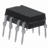
IL300-DEFG Vishay, IL300-DEFG Datasheet - Page 9

IL300-DEFG
Manufacturer Part Number
IL300-DEFG
Description
OPTOCOUPLER HI GAIN WIDE BW 8DIP
Manufacturer
Vishay
Specifications of IL300-DEFG
Mounting Type
Through Hole
Isolation Voltage
5300 Vrms
Number Of Channels
2
Input Type
DC
Voltage - Isolation
5300Vrms
Current Transfer Ratio (min)
0.77% @ 10mA
Current Transfer Ratio (max)
1.18% @ 10mA
Current - Dc Forward (if)
60mA
Output Type
Linear Photovoltaic
Package / Case
8-DIP (0.300", 7.62mm)
Current Transfer Ratio
0.5 % to 1.1 %
Forward Current
10 mA
Maximum Fall Time
1.75 us
Maximum Rise Time
1.75 us
Output Device
PIN Photodiode
Configuration
1 Channel
Maximum Forward Diode Voltage
1.5 V
Maximum Reverse Diode Voltage
5 V
Maximum Input Diode Current
60 mA
Maximum Power Dissipation
210 mW
Maximum Operating Temperature
+ 100 C
Minimum Operating Temperature
- 55 C
No. Of Channels
1
Optocoupler Output Type
Photodiode
Input Current
10mA
Output Voltage
50V
Opto Case Style
DIP
No. Of Pins
8
Gain Db Max
1.181dB
Lead Free Status / RoHS Status
Lead free / RoHS Compliant
Voltage - Output
-
Current - Output / Channel
-
Vce Saturation (max)
-
Lead Free Status / Rohs Status
Lead free / RoHS Compliant
Other names
751-1293-5
IL300-DEFGGI
IL300-DEFGGI
IL300-DEFGGI
IL300-DEFGGI
Available stocks
Company
Part Number
Manufacturer
Quantity
Price
Company:
Part Number:
IL300-DEFG
Manufacturer:
Vishay
Quantity:
2 000
The isolated amplifier provides the PWM control sig-
nal which is derived from the output supply voltage.
Figure 16 more closely shows the basic function of
the amplifier.
The control amplifier consists of a voltage divider and
a non-inverting unity gain stage. The TDA4918 data
sheet indicates that an input to the control amplifier is
a high quality operational amplifier that typically
requires a +3.0 V signal. Given this information, the
amplifier circuit topology shown in Figure 18 is
selected.
The power supply voltage is scaled by R1 and R2 so
that there is + 3.0 V at the non-inverting input (Va) of
U1. This voltage is offset by the voltage developed by
photocurrent flowing through R3. This photocurrent is
developed by the optical flux
created by current flowing through the LED. Thus as
the scaled monitor voltage (Va) varies it will cause a
change in the LED current necessary to satisfy the dif-
ferential voltage needed across R3 at the inverting
input.
The first step in the design procedure is to select the
value of R3 given the LED quiescent current (IFq) and
the servo gain (K1). For this design, I
ure 4 shows the servo photocurrent at I
be 100 µA. With this data R3 can be calculated.
For best input offset compensation at U1, R2 will
equal R3. The value of R1 can easily be calculated
from the following.
Document Number 83622
Rev. 1.5, 24-Mar-05
VISHAY
iil300_16
To Control
R3 =
R1 = R2
Input
V
I
PI
b
(
=
Figure 16. Isolated Control Amplifier
V
100 A
V a
MONITOR
3 V
ISO
AMP
+1
+
-
= 30 K
- 1
)
R2
R1
17165
Voltage
Monitor
17164
Fq
= 12 mA. Fig-
Fq
is found to
The value of R5 depends upon the IL300 Transfer
Gain (K3). K3 is targeted to be a unit gain device,
however to minimize the part to part Transfer Gain
variation, Infineon offers K3 graded into ± 5 % bins.
R5 can determined using the following equation,
Or if a unity gain amplifier is being designed (VMON-
ITOR = VOUT, R1 = 0), the equation simplifies to:
R5 =
R5 =
V
MONITOR
V
K3
R3
OUT
R3(R1 + R2)
17190
R2K3
Vishay Semiconductors
17166
www.vishay.com
IL300
9


