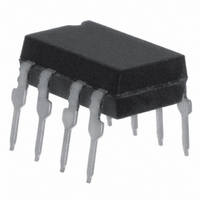
IL300-DEFG Vishay, IL300-DEFG Datasheet - Page 9

IL300-DEFG
Manufacturer Part Number
IL300-DEFG
Description
OPTOCOUPLER HI GAIN WIDE BW 8DIP
Manufacturer
Vishay
Specifications of IL300-DEFG
Mounting Type
Through Hole
Isolation Voltage
5300 Vrms
Number Of Channels
2
Input Type
DC
Voltage - Isolation
5300Vrms
Current Transfer Ratio (min)
0.77% @ 10mA
Current Transfer Ratio (max)
1.18% @ 10mA
Current - Dc Forward (if)
60mA
Output Type
Linear Photovoltaic
Package / Case
8-DIP (0.300", 7.62mm)
Current Transfer Ratio
0.5 % to 1.1 %
Forward Current
10 mA
Maximum Fall Time
1.75 us
Maximum Rise Time
1.75 us
Output Device
PIN Photodiode
Configuration
1 Channel
Maximum Forward Diode Voltage
1.5 V
Maximum Reverse Diode Voltage
5 V
Maximum Input Diode Current
60 mA
Maximum Power Dissipation
210 mW
Maximum Operating Temperature
+ 100 C
Minimum Operating Temperature
- 55 C
No. Of Channels
1
Optocoupler Output Type
Photodiode
Input Current
10mA
Output Voltage
50V
Opto Case Style
DIP
No. Of Pins
8
Gain Db Max
1.181dB
Lead Free Status / RoHS Status
Lead free / RoHS Compliant
Voltage - Output
-
Current - Output / Channel
-
Vce Saturation (max)
-
Lead Free Status / Rohs Status
Lead free / RoHS Compliant
Other names
751-1293-5
IL300-DEFGGI
IL300-DEFGGI
IL300-DEFGGI
IL300-DEFGGI
Available stocks
Company
Part Number
Manufacturer
Quantity
Price
Company:
Part Number:
IL300-DEFG
Manufacturer:
Vishay
Quantity:
2 000
Document Number: 83622
Rev. 1.6, 10-Nov-10
TABLE 2 - OPTOLINEAR AMPLIEFIERS
AMPLIFIER
Non-inverting
Inverting
Fig. 16 - Amplitude and Phase Power Supply Control
iil300_21
- 2
- 4
- 6
- 8
2
0
10
3
Non-inverting
Non-inverting
F - Frequency (Hz)
Inverting
Inverting
INPUT
10
4
iil300_22
V in
R1
R1
V in
For technical questions, contact:
Non-inverting input
10
5
R2
R2
Non-inverting
Non-inverting
Inverting input
dB
Phase
- V ref1
+ V ref1
OUTPUT
3
2
3
2
Inverting
Inverting
+
R3
+
R3
–
–
4
4
Fig. 17 - Non-inverting and Inverting Amplifiers
Linear Optocoupler, High Gain
7
7
10
- V cc
20 pF
V cc
Vcc
Stability, Wide Bandwidth
V cc
6
- 45
- 90
- 135
- 180
6
6
45
0
20 pF
+V cc
100 Ω
100 Ω
- V cc
- V cc
+ V cc
V
V
V
V
1
2
3
4
1
2
3
4
OUT
IN
OUT
IN
V
V
V
V
OUT
IN
OUT
IN
IL 300
IL 300
=
=
optocoupleranswers@vishay.com
=
=
K3 R4 R2 (R5 + R6)
- K3 R4 R2 (R5 + R6)
R3 R5 (R1 + R2)
The same procedure can be used to design isolation
amplifiers that accept bipolar signals referenced to ground.
These amplifiers circuit configurations are shown in
figure 17. In order for the amplifier to respond to a signal that
swings above and below ground, the LED must be pre
biased from a separate source by using a voltage reference
source (V
following equation.
R3 R5 (R1 + R2)
Non-inverting output
R3 (R1 + R2)
R3 (R1 + R2)
GAIN
- K3 R4 R2
8
7
6
5
8
7
6
5
Inverting output
K3 R4 R2
V cc
Vcc
+ V ref2
R4
2
3
3
2
+ V ref2
R5
ref1
R3 =
+
+
–
–
R4
). In these designs, R3 can be determined by the
R6
7
7
- V cc
4
4
Vcc
V cc
- V cc
V
I
P1
ref1
Vo
6
6
V out
Vishay Semiconductors
=
K1I
V
V
V
ref1
ref2
ref2
Fq
V
V
ref2
ref2
=
=
=
- V
=
V
ref1
OFFSET
ref1
- V
V
ref1
R4 (R5 + R6) K3
ref1
R4 (R5 + R6) K3
R3
R3
R3 R6
R3 R6
R4 K3
R4 K3
17098
www.vishay.com
IL300
9


