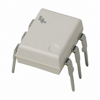
H11AV2AVM Fairchild Optoelectronics Group, H11AV2AVM Datasheet

H11AV2AVM
Specifications of H11AV2AVM
Related parts for H11AV2AVM
H11AV2AVM Summary of contents
Page 1
H11AV1M, H11AV1AM, H11AV2M, H11AV2AM Phototransistor Optocouplers Features H11AV1M and H11AV2M feature 0.3" input-output lead spacing H11AV1AM and H11AV2AM feature 0.4" input-output lead spacing UL recognized (File #E90700, Vol. 2) VDE recognized (File #102497) Add option V (e.g., H11AV1AVM) Applications Power ...
Page 2
Absolute Maximum Ratings Stresses exceeding the absolute maximum ratings may damage the device. The device may not function or be operable above the recommended operating conditions and stressing the parts to these levels is not recommended. In addition, extended exposure ...
Page 3
Electrical Characteristics Individual Component Characteristics Symbol Parameter EMITTER V Input Forward Voltage ( Reverse Leakage Current R DETECTOR BV Collector-Emitter Breakdown Voltage CEO BV Collector-Base Breakdown Voltage CBO BV Emitter-Collector Breakdown Voltage ECO I Collector-Emitter Dark Current CEO ...
Page 4
Safety and Insulation Ratings As per IEC 60747-5-2, this optocoupler is suitable for “safe electrical insulation” only within the safety limit data. Compliance with the safety ratings shall be ensured by means of protective circuits. Symbol Installation Classifications per DIN ...
Page 5
Typical Performance Curves Fig. 1 LED Forward Voltage vs. Forward Current 1.8 1.7 1.6 1.5 1.4 T 1.3 T 1.2 T 1.1 1 – LED FORWARD CURRENT (mA) F Fig. 3 Normalized CTR vs. Ambient Temperature 1.4 ...
Page 6
Typical Performance Curves Fig. 7 Switching Speed vs. Load Resistor 1000 100 T off 0.1 0 – ...
Page 7
Package Dimensions Through Hole 8.13–8. 6.10–6.60 Pin 5.08 (Max.) 0.25–0.36 3.28–3.53 0.38 (Min.) 2.54–3.81 2.54 (Bsc) (0.86) 0.41–0.51 1.02–1.78 0.76–1.14 Surface Mount 6.10–6.60 8.43–9.90 3.28–3.53 5.08 (Max.) 0.38 (Min.) Note: All dimensions in mm. ©2005 ...
Page 8
Ordering Information Option No option S SR2 SR2V Marking Information Definitions *Note – Parts that do not have the ‘V’ option (see definition 3 above) that are marked with date ...
Page 9
Tape Dimensions 4.5 0.20 0.30 0.05 21.0 0.1 0.1 MAX User Direction of Feed Note: All dimensions are in millimeters. Reflow Soldering Profile 300 280 260 240 220 200 180 160 C 140 120 100 ...
Page 10
TRADEMARKS The following includes registered and unregistered trademarks and service marks, owned by Fairchild Semiconductor and/or its global subsidiaries, and is not intended exhaustive list of all such trademarks. Auto-SPM™ F-PFS™ Build it Now™ FRFET CorePLUS™ Global ...


