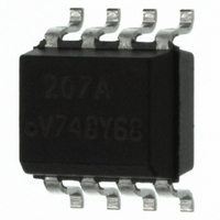
SFH6318T Vishay, SFH6318T Datasheet - Page 3

SFH6318T
Manufacturer Part Number
SFH6318T
Description
OPTOCOUPLER 100KBD 2600% 8SOIC
Manufacturer
Vishay
Datasheet
1.SFH6318T.pdf
(6 pages)
Specifications of SFH6318T
Isolation Voltage
4000 Vrms
Voltage - Isolation
4000Vrms
Number Of Channels
1, Unidirectional
Current - Output / Channel
60mA
Propagation Delay High - Low @ If
2µs @ 1.6mA
Current - Dc Forward (if)
20mA
Input Type
DC
Output Type
Logic
Mounting Type
Surface Mount
Package / Case
8-SOIC (3.9mm Width)
Current Transfer Ratio (max)
2600% @ 1.6mA
Current Transfer Ratio (min)
300% @ 1.6mA
Output Device
Photodarlington
Configuration
1 Channel
Current Transfer Ratio
2600 %
Maximum Baud Rate
100 KBps
Maximum Forward Diode Voltage
1.7 V
Maximum Reverse Diode Voltage
3 V
Maximum Input Diode Current
20 mA
Maximum Power Dissipation
150 mW
Maximum Operating Temperature
+ 100 C
Minimum Operating Temperature
- 55 C
No. Of Channels
1
Optocoupler Output Type
Photodarlington
Input Current
1.6mA
Output Voltage
7V
Opto Case Style
SOIC
No. Of Pins
8
Propagation Delay Low-high
35µs
Lead Free Status / RoHS Status
Lead free / RoHS Compliant
Voltage - Output
-
Vce Saturation (max)
-
Lead Free Status / RoHS Status
Lead free / RoHS Compliant, Lead free / RoHS Compliant
Notes
• Minimum and maximum values are testing requirements. Typical values are characteristics of the device and are the result of engineering
(1)
(2)
Note
• T
Note
(1)
Document Number: 83678
Rev. 1.8, 19-Oct-10
ELECTRICAL CHARACTERISTICS (T
PARAMETER
COUPLER
Capacitance (input to output)
Input capacitance
Resistance (input to output)
CURRENT TRANSFER RATIO
PARAMETER
Current transfer ratio
SWITCHING CHARACTERISTICS (T
PARAMETER
Propagation delay time to logic
low at output
Propagation delay time to logic
low at output
Propagation delay time to logic
low at output
Propagation delay time to logic
high at output
Propagation delay time to logic
high at output
Propagation delay time to logic
high at output
evaluation. Typical values are for information only and are not part of the testing requirements.
T
Pin 7 open.
Device considered a two-terminal device: pins 1, 2, 3 and 4 shorted together and pins 5, 6, 7 and 8 shorted together.
DC current transfer ratio is defined as the ratio of output collector current, I
Pin 7 open. Using a resistor between pin 5 and 7 will decrease gain and delay time.
amb
amb
= 0 °C to 70 °C. Typical values are specified at T
= 0 °C to 70 °C. Typical values are specified at T
isfh6318t_01
10 % duty cycle
1/f < 100 µs
I
Pulse
generator
Z O = 5 0 Ω
t
F
r
(2)
= 5 n s
= monitor
(2)
R
I
F
m
(2)
(2)
1
2
3
4
I
I
I
F
F
F
For technical questions, contact:
I
I
I
I
= 1.6 mA, V
= 0.5 mA, V
= 1.6 mA, V
F
F
I
F
F
I
F
F
V
V
= 1.6 mA, R
= 0.5 mA, R
= 1.6 mA, R
= 0.5 mA, R
IO
TEST CONDITION
= 12 mA, R
= 12 mA, R
IO
= 500 VDC, T
= 500 VDC, T
High Speed Optocoupler, 100 kBd,
TEST CONDITION
TEST CONDITION
f = 1 MHz, V
Low Input Current, High Gain
f = 1 MHz
O
O
O
amb
L
L
L
L
L
L
= 0.4 V, V
= 0.4 V, V
= 0.4 V, V
amb
8
7
6
5
= 2.2 kΩ
= 4.7 kΩ
= 270 Ω
= 2.2 kΩ
= 4.7 kΩ
= 270 Ω
Fig. 1 - Switching Test Circuit
= 25 °C, unless otherwise specified)
amb
amb
amb
amb
= 25 °C, unless otherwise specified)
F
= 0
= 100 °C
= 25 °C.
= 25 °C.
= 25 °C
CC
CC
CC
0.1 µF
= 4.5 V SFH6318T
= 4.5 V SFH6319T
= 4.5 V SFH6319T
R
SFH6318T
SFH6319T
SFH6319T
SFH6318T
SFH6319T
SFH6319T
L
PART
C
optocoupleranswers@vishay.com
L
= 15 pF
+ 5 V
V
O
SYMBOL
PART
O
C
C
R
R
, to the forward LED input current, I
IO
IN
IO
IO
SYMBOL
(non-saturated
t
t
t
t
t
t
(saturated
PHL
PHL
PHL
PLH
PLH
PLH
response)
response)
V
I
V
0
SYMBOL
O
t
PHL
CTR
CTR
CTR
MIN.
MIN.
SFH6318T, SFH6319T
90 %
10 %
1.5 V
t
f
Vishay Semiconductors
MIN.
300
400
500
TYP.
10
10
0.6
25
TYP.
12
11
t
0.6
1.5
PLH
2
6
2
4
10 %
1600
2000
1600
TYP.
90 %
F
times 100 %. Pin 7 open.
1.5 V
MAX.
MAX.
t
r
10
25
35
60
1
7
MAX.
2600
3500
2600
V
5 V
OL
www.vishay.com
5 V
UNIT
UNIT
pF
pF
UNIT
Ω
Ω
μs
μs
μs
μs
μs
μs
%
%
%
3


