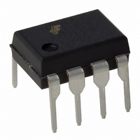
HCPL3700V Fairchild Optoelectronics Group, HCPL3700V Datasheet - Page 4

HCPL3700V
Manufacturer Part Number
HCPL3700V
Description
OPTOCOUPLER AD/DC LOGIC 8-DIP
Manufacturer
Fairchild Optoelectronics Group
Datasheet
1.HCPL3700.pdf
(9 pages)
Specifications of HCPL3700V
Voltage - Isolation
2500Vrms
Number Of Channels
1, Unidirectional
Current - Output / Channel
30mA
Propagation Delay High - Low @ If
6µs
Input Type
AC, DC
Output Type
Logic
Mounting Type
Through Hole
Package / Case
8-DIP
Voltage - Output
20V
Lead Free Status / RoHS Status
Lead free / RoHS Compliant
Current - Dc Forward (if)
-
Vce Saturation (max)
-
Current Transfer Ratio (max)
-
Current Transfer Ratio (min)
-
10. The 2500 V
11. AC voltage is instantaneous voltage for V
12. All typicals at T
1. Derate linearly above 70°C free-air temperature at a rate of 1.8 mW/°C.
2. Derate linearly above 70°C free-air temperature at a rate of 2.5 mW/°C.
3. Derate linearly above 70°C free-air temperature at a rate of 0.6 mA/°C.
4. Derate linearly above 70°C free-air temperature at a rate of 1.9 mW/°C.
5. Logic low output level at pin 6 occurs when V
6. T
7. Common mode transient immunity in logic high level is the maximum tolerable (positive) dV
8. In applications where dV
9. Device is considered a two terminal device: Pins 1, 2, 3 and 4 are shorted together and Pins 5, 6, 7 and 8 are shorted together.
NOTES
occurs when V
on the leading edge of the output pulse. T
(Refer to Fig. 9)
common mode pulse signal V
immunity in logic low level is the maximum tolerable (negative) dV
to assure that the output will remain in a logic low state (i.e., V
protect the detector chip from destructive surge currents. The recommended value for R
V
PHL
CC
(between pin 8 and V
propagation delay is measured from the 2.5 V level of the leading edge of a 5.0 V input pulse (1 µs rise time) to the 1.5 V level
RMS
IN
A
/1 min. capability is validated by 3.0 kV
"V
= 25°C, V
TH-
and when V
cm
CC
CC
/dt may exceed 50,000 V/µs (Such as static discharge), a series resistor, R
) with a minimum value of 240 $.
CM
= 5 V unless otherwise specified.
, to assure that the output will remain in a logic high state (i.e., V
IN
&V
TH+
TH+
PLH
once V
& V
IN
propagation delay is measured on the trailing edges of the input and output pulse.
!V
TH-
TH+
.
IN
decreases below V
and when V
RMS
/1 sec. dielectric voltage withstand test.
O
&0.8 V). (Refer to Fig.10)
cm
AC/DC TO LOGIC INTERFACE
IN
%V
/dt on the trailing edge of the common mode pulse signal, V
TH-
TH-.
once V
IN
exceeds V
CC
is 240 $ per volt of allowable drop in
cm
/dt on the leading edge of the
TH+
O
OPTOCOUPLER
%2.0 V). Common mode transient
. Logic high output level at pin 6
CC
, should be included to
HCPL-3700
200003A
CM
,


