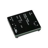
4N25-300E Avago Technologies US Inc., 4N25-300E Datasheet - Page 6

4N25-300E
Manufacturer Part Number
4N25-300E
Description
OPTOCOUPLER PHOTOTRANS 6-SMD GW
Manufacturer
Avago Technologies US Inc.
Datasheet
1.4N25-000E.pdf
(7 pages)
Specifications of 4N25-300E
Number Of Channels
1
Input Type
DC
Voltage - Isolation
2500Vrms
Current Transfer Ratio (min)
20% @ 10mA
Voltage - Output
30V
Current - Output / Channel
100mA
Current - Dc Forward (if)
10mA
Vce Saturation (max)
500mV
Output Type
Transistor with Base
Mounting Type
Surface Mount, Gull Wing
Package / Case
6-SMD Gull Wing
No. Of Channels
1
Optocoupler Output Type
Phototransistor
Input Current
10mA
Output Voltage
30V
Opto Case Style
SMD
No. Of Pins
6
Isolation Voltage
2.5kV
Output Device
Transistor With Base
Number Of Elements
1
Reverse Breakdown Voltage
6V
Forward Voltage
1.5V
Forward Current
80mA
Collector-emitter Voltage
30V
Package Type
PDIP SMD
Collector Current (dc) (max)
100mA
Power Dissipation
250mW
Collector-emitter Saturation Voltage
0.5V
Pin Count
6
Mounting
Surface Mount
Operating Temp Range
-55C to 100C
Operating Temperature Classification
Industrial
Lead Free Status / RoHS Status
Lead free / RoHS Compliant
Current Transfer Ratio (max)
-
Lead Free Status / Rohs Status
Compliant
Figure 4. Current transfer ratio vs. forward current.
Figure 7. Collector-emitter saturation voltage vs.
temperature.
Figure 10. Frequency response.
6
-10
-15
-20
50
40
30
20
10
-5
0
5
0
0.1
0.3
0.2
0.1
0.5
0
-55
0.2
V
T
I
F
T
A
1
CE
R
500 kΩ
A
– FORWARD CURRENT – mA
BE
= 25°C
– AMBIENT TEMPERATURE – °C
I
R
R
= 10 V
I
2
F
-25
0.5
C
f – FREQUENCY – kHz
R
L
L
=
= 50 mA
L
= 2 mA
= 10 kΩ
= 100 Ω
= 1 kΩ
1
5
4N25 fig 10
4N25 fig 4
0
10
2
4N25 fig 7
20
25
5
100 kΩ
10
50
V
I
T
50
C
100 200
20
A
CE
= 2 mA
= 25°C
= 5 V
75
50
100
500
100
Figure 5. Collector current vs. collector-emitter volt-
age.
Figure 8. Collector dark current vs. temperature.
Figure 11. Collector-emitter saturation voltage vs.
forward current.
10
10
10
10
15
10
V
10
10
10
10
5
0
-10
-11
-12
-13
CE
-6
-7
-8
-9
0
5
5
5
5
5
5
5
-55
7
6
5
4
3
2
1
0
T
– COLLECTOR-EMITTER VOLTAGE – V
0
T
A
A
V
= 25°C
-25
CE
– AMBIENT TEMPERATURE – °C
I
F
– FORWARD CURRENT – mA
5
= 10 V
0
5
I
I
I
I
10
4N25 fig 5
F
F
F
F
I
F
4N25 fig 8
4N25 fig 11
= 40 mA
= 30 mA
= 20 mA
= 10 mA
20
= 5 mA
15
40
10
20
80
P
C
T
A
(MAX.)
100
= 25°C
25
15
125
30
Figure 6. Relative current transfer ratio vs. tempera-
ture.
Figure 9. Response time vs. load resistance.
300
200
100
100
0.5
0.2
0.1
50
20
10
0
0.05
5
2
1
-55
T
A
V
I
T
C
R
CE
A
– AMBIENT TEMPERATURE – °C
-25
0.1
= 2 mA
L
= 25°C
– LOAD RESISTANCE – kΩ
= 10 V
0.2
0
0.5
4N25 fig 6
4N25 fig 9
25
1
2
50
5
V
I
F
CE
= 10 mA
10
75
= 10 V
tf
tr
td
ts
20 50
100


