HCNW4504#500 Avago Technologies US Inc., HCNW4504#500 Datasheet
HCNW4504#500
Specifications of HCNW4504#500
Available stocks


Related parts for HCNW4504#500


HCNW4504#500 Summary of contents
Page 1
HCPL-4504/J454/0454, HCNW4504 High CMR, High Speed Optocouplers Data Sheet Lead (Pb) Free RoHS 6 fully compliant RoHS 6 fully compliant options available; -xxxE denotes a lead-free product Description The HCPL-4504 and HCPL-0454 contain a GaAsP LED while the HCPL-J454 and ...
Page 2
Ordering Information HCPL-0454, HCPL-4504 and HCPL-J454 are UL Recognized with 3750 Vrms for 1 minute per UL1577. HCNW4504 is UL Recognized with 5000 Vrms for 1 minute per UL1577. HCPL-0454, HCPL-4504, HCPL-J454 and HCNW4504 are approved under CSA Component Acceptance ...
Page 3
Package Outline Drawings HCPL-4504 Outline Drawing 9.65 ± 0.25 (0.380 ± 0.010 TYPE NUMBER A XXXXZ R U YYWW 1.19 (0.047) MAX. 3.56 ± 0.13 (0.140 ± 0.005) 1.080 ± 0.320 (0.043 ± 0.013) ...
Page 4
Package Outline Drawings HCPL-J454 Outline Drawing 9.80 ± 0.25 (0.386 ± 0.010 TYPE NUMBER A XXXX R U YYWW 1.19 (0.047) MAX. 3.56 ± 0.13 (0.140 ± 0.005) 1.080 ± 0.320 (0.043 ± 0.013) ...
Page 5
HCPL-J454-400E/600E Widelead Gullwing Surface Mount Outline Drawing 9.80 ±0.25 0.386 ±0.010 TYPE NUMBER A XXXX DATE CODE YYWW R [0.65] 0.025 MAX [1.19] 0.047 MAX. [1.080] 0.320 0.043 0.013 0.100 DIMENSIONS IN [MILLIMETERS] INCHES OPTION NUMBERS 400 AND 600 NOT ...
Page 6
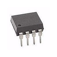
HCNW4504 Outline Drawing (8-Pin Widebody Package) 11.15 ± 0.15 (0.442 ± 0.006 HCNWXXXX YYWW 2.54 (0.100) TYP. 1.78 ± 0.15 (0.070 ± 0.006) HCNW4504 Gull Wing Surface Mount Option 300 Outline Drawing 11.15 ...
Page 7
Solder Refl ow Temperature Profi le 300 PREHEATING RATE 3 ° °C/–0.5 °C/SEC. REFLOW HEATING RATE 2.5 °C ± 0.5 °C/SEC. 200 160 °C 150 °C 140 °C 3 ° °C/–0.5 °C 100 ROOM TEMPERATURE 0 ...
Page 8
Regulatory Information The devices contained in this data sheet have been approved by the following agencies: Agency/Standard Underwriters Laboratories (UL) UL1577 Recognized under UL1577, Component Recognition Program, Category FPQU2, File E55361 Canadian Standards Association (CSA) Component Acceptance File CA88324 Notice ...
Page 9
IEC/EN/DIN EN 60747-5-2 Insulation Related Characteristics Description Installation classifi cation per DIN VDE 0110/1.89, Table 1 for rated mains voltage ≤150 V rms for rated mains voltage ≤300 V rms for rated mains voltage ≤450 V rms for rated mains ...
Page 10
Absolute Maximum Ratings Parameter Storage Temperature Operating Temperature Average Forward Input Current Peak Forward Input Current (50% duty cycle pulse width) Peak Transient Input Current (≤1 μs pulse width, 300 pps) Reverse LED Input Voltage (Pin 3-2) Input ...
Page 11
Electrical Specifi cations (DC) Over recommended temperature (T Parameter Symbol Device Current CTR HCPL-4504 Transfer HCPL-0454 Ratio HCPL-J454 HCNW4504 Current CTR HCPL-4504 Transfer HCPL-0454 Ratio HCPL-J454 HCNW4504 Logic Low V HCPL-4504 OL Output HCPL-0454 Voltage HCPL-J454 HCNW4504 Logic High I ...
Page 12
AC Switching Specifi cations Over recommended temperature (T = 0°C to 70°C) unless otherwise specifi ed. A Parameter Symbol Device Propagation Delay t PHL Time to Logic Low at Output t PHL HCPL- J454 Others 0.1 Propagation Delay t PLH ...
Page 13
Package Characteristics Over recommended temperature (T A Parameter Symbol Device Input-Output V HCPL-4504 ISO Momentary HCPL-0454 Withstand HCPL-J454 Voltage† HCPL-4504 Option 020 HCNW4504 Input-Output R HCPL-4504 I-O Resistance HCPL-0454 HCPL-J454 HCNW4504 Capacitance C HCPL-4504 I-O (Input-Output) HCPL-0454 HCPL-J454 HCNW4504 All ...
Page 14
HCPL-4504/0454 25° 5 – OUTPUT VOLTAGE – ...
Page 15
HCPL-4504/0454 1.1 1.0 0.9 NORMALIZED 0 25°C A 0.7 0.6 -60 -40 - 100 120 T – TEMPERATURE ...
Page 16
HCPL-4504/0454 0. 5 1.9 kΩ 1.5 V THHL THLH t PLH 10% DUTY CYCLE 0.35 t PHL 0.30 0.25 0. ...
Page 17
HCPL-4504 OPTION 060/HCPL-J454 800 P (mW) S 700 I (mA) for HCPL-4504 S OPTION 060 600 I (mA) for HCPL-J454 S 500 400 300 (230) 200 100 100 125 150 175 200 T – CASE ...
Page 18
Figure 17. LED delay and dead time diagram. Power Inverter Dead Time and Propagation Delay Specifi ca- tions The HCPL-4504/0454/J454 and HCNW4504 include a specifi ca tion intended to help designers minimize “dead time” in their power inverter designs. The ...
Page 19
The LED signal to turn on Q2 should be delayed enough so that an optocoupler with the very fastest turn-on propagation delay (t ) will never turn on before an PHLmin optocoupler with the very slowest turn-off propagation delay (t ...