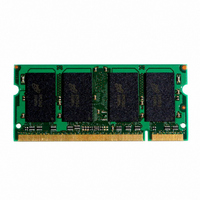
MT18VDDF12872HG-40BD1 Micron Technology Inc, MT18VDDF12872HG-40BD1 Datasheet - Page 13

MT18VDDF12872HG-40BD1
Manufacturer Part Number
MT18VDDF12872HG-40BD1
Description
MODULE DDR SDRAM 1GB 200-SODIMM
Manufacturer
Micron Technology Inc
Datasheet
1.MT18VDDF12872HY-40BF1.pdf
(26 pages)
Specifications of MT18VDDF12872HG-40BD1
Memory Type
DDR SDRAM
Memory Size
1GB
Speed
200MHz
Package / Case
200-SODIMM
Lead Free Status / RoHS Status
Contains lead / RoHS non-compliant
Other names
557-1116
Table 12: I
DDR SDRAM devices only;
Notes: 1–5, 8, 10, 12, 46; notes appear on pages 16–18; 0°C
pdf: 09005aef80e4880c, source: 09005aef80e487d7
DDAF18C128x72HG.fm - Rev. A 10/04 EN
PARAMETER/CONDITION
OPERATING CURRENT: One device bank; Active-Precharge;
t
and control inputs changing once every two clock cycles
OPERATING CURRENT: One device bank; Active-Read-Precharge; Burst = 4;
t
changing once per clock cycle
PRECHARGE POWER-DOWN STANDBY CURRENT: All device banks idle;
Power-down mode;
IDLE STANDBY CURRENT: CS# = HIGH; All device banks are idle;
(MIN);
cycle. V
ACTIVE POWER-DOWN STANDBY CURRENT: One device bank active; Power-
down mode;
ACTIVE STANDBY CURRENT: CS# = HIGH; CKE = HIGH;
t
clock cycle; Address and other control inputs changing once per clock cycle
OPERATING CURRENT: Burst = 2;
active; Address and control inputs changing once per clock cycle;
(MIN);
OPERATING CURRENT: Burst = 2; Writes; Continuous burst; One device bank
active; Address and control inputs changing once per clock cycle;
(MIN); DQ, DM, and DQS inputs changing twice per clock cycle
AUTO REFRESH BURST CURRENT:
SELF REFRESH CURRENT: CKE
OPERATING CURRENT: Four device bank interleaving READs
auto precharge,
control inputs change only during Active READ, or WRITE commands
NOTE:
CK =
RC =
RC =
a: Value calculated as one module rank in this operating condition, and all other module ranks in I
b: Value calculated reflects all module ranks in this operating condition.
t
t
t
RAS (MAX);
CK (MIN); DQ, DM and DQS inputs changing once per clock cycle; Address
RC (MIN);
I
CKE = HIGH; Address and other control inputs changing once per clock
OUT
IN
= V
= 0mA
REF
t
CK =
DD
t
for DQ, DQS, and DM
RC = minimum
t
CK =
t
CK =
t
CK (MIN); CKE = LOW
Specifications and Conditions – 1GB
t
CK =
t
CK (MIN); I
t
CK (MIN); DQ, DM and DQS inputs changing twice per
t
CK (MIN);
0.2V
t
RC allowed;
Reads; Continuous burst; One device bank
OUT
CKE = (LOW)
= 0mA; Address and control inputs
t
CK =
t
CK (MIN); Address and
t
t
REFC =
REFC = 7.8125µs
One device bank active
13
T
A
t
t
RFC (MIN)
RC =
(Burst = 4) with
+70°C; V
t
t
CK =
CK =
t
CK =
t
RC (MIN);
Micron Technology, Inc., reserves the right to change products or specifications without notice.
t
t
CK
CK
t
DD
CK
1GB (x72, ECC, DR) PC3200
, V
DD
;
Q = +2.6V ±0.1V
200-PIN DDR SODIMM
I
I
I
I
I
I
I
DD4W
SYM
DD3N
I
DD5A
I
I
I
I
DD2P
DD2F
DD3P
DD4R
DD0
DD1
DD5
DD6
DD7
a
a
b
b
a
b
b
b
b
a
b
a
MAX
1,440
1,710
1,080
1,755
1,800
6,210
4,095
-40B
990
810
198
90
90
DD
2p (CKE LOW) mode.
UNITS
©2004 Micron Technology, Inc.
mA
mA
mA
mA
mA
mA
mA
mA
mA
mA
mA
mA
21, 28, 42
21, 28, 42
NOTES
20, 40
20, 40
20, 40
20, 42
24, 42
20, 41
43
20
9


