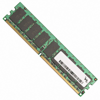
MT9HTF6472AY-40ED4 Micron Technology Inc, MT9HTF6472AY-40ED4 Datasheet - Page 13

MT9HTF6472AY-40ED4
Manufacturer Part Number
MT9HTF6472AY-40ED4
Description
MODULE DDR2 512MB 240-DIMM
Manufacturer
Micron Technology Inc
Specifications of MT9HTF6472AY-40ED4
Memory Type
DDR2 SDRAM
Memory Size
512MB
Speed
400MT/s
Package / Case
240-DIMM
Main Category
DRAM Module
Sub-category
DDR2 SDRAM
Module Type
240RDIMM
Device Core Size
72b
Organization
64Mx72
Total Density
512MByte
Chip Density
512Mb
Access Time (max)
60ps
Maximum Clock Rate
400MHz
Operating Supply Voltage (typ)
1.8V
Operating Current
1.035A
Number Of Elements
9
Operating Supply Voltage (max)
1.9V
Operating Supply Voltage (min)
1.7V
Operating Temp Range
0C to 85C
Operating Temperature Classification
Commercial
Pin Count
240
Mounting
Socket
Lead Free Status / RoHS Status
Lead free / RoHS Compliant
Mode Register (MR)
Burst Length
Burst Type
pdf: 09005aef80e6f860, source: 09005aef80e5b799
HTF9C32_64_128x72AG_2.fm - Rev. C 6/05 EN
The mode register is used to define the specific mode of operation of the DDR2 SDRAM
device. This definition includes the selection of a burst length, burst type, CAS latency,
operating mode, DLL reset, write recovery, and power-down mode as shown in Figure 5,
Mode Register (MR) Definition. Contents of the mode register can be altered by re-exe-
cuting the LOAD MODE (LM) command. If the user chooses to modify only a subset of
the MR variables, all variables (M0–M14) must be programmed when the LOAD MODE
command is issued.
The mode register is programmed via the LM command (bits BA0–BA1/BA2 all = 0) and
other bits (M0–M13 or M0–M14) will retain the stored information until it is pro-
grammed again or the device loses power (except for bit M8, which is self-clearing).
Reprogramming the mode register will not alter the contents of the memory array, pro-
vided it is performed correctly.
The LOAD MODE command can only be issued (or reissued) when all banks are in the
precharged state. The controller must wait the specified time
subsequent operations such as an ACTIVE command. Violating either of these require-
ments will result in unspecified operation.
Burst length is defined by bits M0–M2 as shown in Figure 5, Mode Register (MR) Defini-
tion. Read and write accesses to the DDR2 SDRAM device are burst-oriented, with the
burst length being programmable to either four or eight. The burst length determines
the maximum number of column locations that can be accessed for a given READ or
WRITE command.
When a READ or WRITE command is issued, a block of columns equal to the burst
length is effectively selected. All accesses for that burst take place within this block,
meaning that the burst will wrap within the block if a boundary is reached. The block is
uniquely selected by A2–Ai when the burst length is set to four and by A3–Ai when the
burst length is set to eight (where Ai is the most significant column address bit for a
given configuration). The remaining (least significant) address bit(s) is (are) used to
select the starting location within the block. The programmed burst length applies to
both READ and WRITE bursts.
Accesses within a given burst may be programmed to be either sequential or interleaved.
The burst type is selected via bit M3 as shown in Figure 5, Mode Register (MR) Defini-
tion. The ordering of accesses within a burst is determined by the burst length, the burst
type, and the starting column address as shown in Table 6, Burst Definition, on page 15.
DDR2 SDRAM devices support 4-bit burst and 8-bit burst modes only. For 8-bit burst
mode, full interleave address ordering is supported; however, sequential address order-
ing is nibble-based.
256MB, 512MB, 1GB (x72, SR, ECC) 240-Pin DDR2 SDRAM UDIMM
13
Micron Technology, Inc., reserves the right to change products or specifications without notice.
©2003, 2004, 2005 Micron Technology, Inc. All rights reserved.
t
MRD before initiating any
Mode Register (MR)


