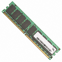
MT9HTF6472AY-40ED4 Micron Technology Inc, MT9HTF6472AY-40ED4 Datasheet - Page 19

MT9HTF6472AY-40ED4
Manufacturer Part Number
MT9HTF6472AY-40ED4
Description
MODULE DDR2 512MB 240-DIMM
Manufacturer
Micron Technology Inc
Specifications of MT9HTF6472AY-40ED4
Memory Type
DDR2 SDRAM
Memory Size
512MB
Speed
400MT/s
Package / Case
240-DIMM
Main Category
DRAM Module
Sub-category
DDR2 SDRAM
Module Type
240RDIMM
Device Core Size
72b
Organization
64Mx72
Total Density
512MByte
Chip Density
512Mb
Access Time (max)
60ps
Maximum Clock Rate
400MHz
Operating Supply Voltage (typ)
1.8V
Operating Current
1.035A
Number Of Elements
9
Operating Supply Voltage (max)
1.9V
Operating Supply Voltage (min)
1.7V
Operating Temp Range
0C to 85C
Operating Temperature Classification
Commercial
Pin Count
240
Mounting
Socket
Lead Free Status / RoHS Status
Lead free / RoHS Compliant
Figure 7:
DQS# Enable/Disable
pdf: 09005aef80e6f860, source: 09005aef80e5b799
HTF9C32_64_128x72AG_2.fm - Rev. C 6/05 EN
Extended Mode Register Definition
The DQS# enable function is defined by bit E10. When enabled (bit E10 = 0), DQS# is the
complement of the differential data strobe pair DQS/DQS#. When disabled (bit E10 = 1),
DQS is used in a single-ended mode and the DQS# pin is disabled. This function is also
used to enable/disable RDQS#. If RDQS is enabled (E11 = 1) and DQS# is enabled (E10 =
0), then both DQS# and RDQS# will be enabled. RDQS/RDQS# is supported only on
RDIMMs using x8 DDR2 SDRAM devices.
256MB Address Bus
512MB Address Bus
1GB Address Bus
BA2
E15
16
0
0
0
1
1
BA1
15
BA1
E14
256MB, 512MB, 1GB (x72, SR, ECC) 240-Pin DDR2 SDRAM UDIMM
EMR
15
EMR
0
1
0
1
E12
14
0
1
BA1
14
BA0
14
BA0
EMR
Extended Mode Register (EMRS2)
Extended Mode Register (EMRS3)
E9
Extended Mode Register (EMRS)
0
0
0
1
1
E11
0
1
Disabled
Outputs
Enabled
13
13
0
BA0
A13
13
0
Mode Register Set (MRS)
E8
A13
RDQS Enable
0
0
1
0
1
E10
Disabled
Reserved
out
out
0
1
out
Mode Register Set
12
12
E7
A12 A11
A12 A11
12
0
1
0
0
1
A12 A11
DQS# Enable
RDQS
RDQS
RDQS
Disable
Enable
OCD Operation
OCD Not Supported
Reserved
Reserved
Reserved
OCD default state
11
11
11
DQS#
DQS#
DQS#
10
10
10
A10
A10
A10
OCD Program
OCD Program
OCD Program
9
9
A9
A9
9
A9
E6
0
0
1
1
8
8
A8
A8
8
A8
E2
†
0
1
0
1
7
7
†
7
A7 A6 A5 A4 A3
A7 A6 A5 A4 A3
A7 A6 A5 A4 A3
Rtt (nominal)
R
Rtt Disabled
Rtt
Rtt
TT
† During initialization, all three bits must be set to ‘1’
‡ Available on -667 speed grade parts only.
150Ω
6
6
75Ω
50Ω ‡
6
for OCD Default State, then must be set to ‘0’
before initialization is finished, as detailed in the
initialization procedure.
Posted CAS# R
Posted CAS# Rtt
Posted CAS# Rtt
5
5
5
19
E5
0
0
0
0
1
1
1
1
4
4
4
E4
0
0
1
1
0
0
1
1
3
3
3
E3
0
1
0
1
0
1
0
1
TT
2
2
2
A2 A1 A0
A2 A1 A0
Posted CAS# Additive Latency (AL)
A2 A1 A0
ODS
ODS
ODS
E1
0
1
1
1
1
Micron Technology, Inc., reserves the right to change products or specifications without notice.
DLL
DLL
Full Strength
Reduced Strength
DLL
E0
0
0
0
1
0
Output Drive Strength
Disable (Test/Debug)
Reserved
Reserved
Reserved
Extended Mode
Register (Ex)
Extended Mode
Register (Ex)
Enable (Normal)
Address Bus
Address Bus
Extended Mode
Register (Ex)
Address Bus
0
1
2
3
4
DLL Enable
©2003, 2004, 2005 Micron Technology, Inc. All rights reserved.
DQS# Enable/Disable


