MT9HVF6472PY-667D1 Micron Technology Inc, MT9HVF6472PY-667D1 Datasheet - Page 19
MT9HVF6472PY-667D1
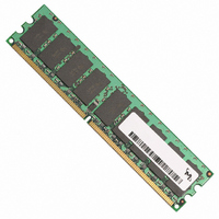
Manufacturer Part Number
MT9HVF6472PY-667D1
Description
MODULE DDR2 512MB 240-DIMM
Manufacturer
Micron Technology Inc
Specifications of MT9HVF6472PY-667D1
Memory Type
DDR2 SDRAM
Memory Size
512MB
Speed
667MT/s
Package / Case
240-DIMM
Main Category
DRAM Module
Sub-category
DDR2 SDRAM
Module Type
240RDIMM
Device Core Size
72b
Organization
64Mx72
Total Density
512MByte
Chip Density
512Mb
Access Time (max)
45ps
Maximum Clock Rate
667MHz
Operating Supply Voltage (typ)
1.8V
Operating Current
1.62A
Number Of Elements
9
Operating Supply Voltage (max)
1.9V
Operating Supply Voltage (min)
1.7V
Operating Temp Range
0C to 90C
Operating Temperature Classification
Commercial
Pin Count
240
Mounting
Socket
Lead Free Status / RoHS Status
Lead free / RoHS Compliant
Other names
557-1208
MT9HVF6472PY-667D1
MT9HVF6472PY-667D1


Table 15: PLL Specifications
CU877 device or equivalent
Table 16: PLL Clock Driver Timing Requirements and Switching Characteristics
PDF: 09005aef81de9391
hvf9c32_64_128x72py.pdf - Rev. E 03/10 EN
Parameter
DC high-level
input voltage
DC low-level
input voltage
Input voltage (limits)
DC high-level
input voltage
DC low-level
input voltage
Input differential-pair
cross voltage
Input differential
voltage
Input differential
voltage
Input current
Output disabled
current
Static supply current
Dynamic supply
Input capacitance
Parameter
Stabilization time
Input clock slew rate
SSC modulation frequency
SSC clock input frequency deviation
PLL loop bandwidth (–3dB from unity gain)
Note:
Symbol
V
V
I
I
DDLD
ID(DC)
ID(AC)
V
V
V
V
I
C
V
V
ODL
DD
I
IH
IN
IH
IX
IN
IL
IL
I
1. PLL timing and switching specifications are critical for proper operation of the DDR2
256MB, 512MB, 1GB (x72, ECC, SR) 240-Pin DDR2 VLP RDIMM
DIMM. This is a subset of parameters for the specific PLL used. Detailed PLL information
is available in JEDEC standard JESD82.
RESET#, CK, CK#
Each input
CK, CK#
CK, CK#
CK, CK#
CK, CK#
CK, CK#
CK, CK#
RESET#
RESET#
RESET#
Pins
N/A
RESET# = V
outputs open (not con-
CK, CK# = 270 MHz, all
Differential input
Differential input
Differential input
Differential input
Differential input
CK = CK# = LOW
nected to PCB)
Symbol
V
V
V
19
I
I
I
Condition
slr(i)
= V
= V
= V
LVCMOS
LVCMOS
or V
t
–
–
–
L
DD
DD
DD
SS
–
IL(DC)
; V
or V
or V
or V
I
Micron Technology, Inc. reserves the right to change products or specifications without notice.
= V
SS
SS
SS
IH(AC)
Register and PLL Specifications
Min
1.0
0.0
2.0
30
(V
–
0.65 × V
0.65 × V
DDQ
–250
Min
–10
100
0.3
/2) - 0.15
0.3
0.6
2
–
–
–
–
DD
DD
© 2006 Micron Technology, Inc. All rights reserved.
Max
–0.5
4.0
15
33
(V
–
0.35 × V
0.35 × V
V
DD
V
V
DD
DD
DD
Max
/2) - 0.15
250
500
300
10
3
–
–
–
+ 0.3
- 0.4
- 0.4
DD
DD
Units
MHz
V/ns
kHz
μs
%
Units
mA
µA
µA
µA
µA
pF
V
V
V
V
V
V
V
V
Related parts for MT9HVF6472PY-667D1
Image
Part Number
Description
Manufacturer
Datasheet
Request
R

Part Number:
Description:
IC SDRAM 64MBIT 133MHZ 54TSOP
Manufacturer:
Micron Technology Inc
Datasheet:

Part Number:
Description:
IC SDRAM 64MBIT 5.5NS 86TSOP
Manufacturer:
Micron Technology Inc
Datasheet:
Part Number:
Description:
IC SDRAM 64MBIT 200MHZ 86TSOP
Manufacturer:
Micron Technology Inc
Datasheet:
Part Number:
Description:
IC SDRAM 64MBIT 133MHZ 54TSOP
Manufacturer:
Micron Technology Inc
Datasheet:
Part Number:
Description:
IC SDRAM 128MBIT 133MHZ 54TSOP
Manufacturer:
Micron Technology Inc
Datasheet:

Part Number:
Description:
IC SDRAM 256MBIT 133MHZ 90VFBGA
Manufacturer:
Micron Technology Inc
Datasheet:
Part Number:
Description:
IC SDRAM 128MBIT 133MHZ 54TSOP
Manufacturer:
Micron Technology Inc
Datasheet:
Part Number:
Description:
IC SDRAM 256MBIT 133MHZ 54TSOP
Manufacturer:
Micron Technology Inc
Datasheet:

Part Number:
Description:
IC DDR SDRAM 512MBIT 6NS 66TSOP
Manufacturer:
Micron Technology Inc
Datasheet:
Part Number:
Description:
IC SDRAM 128MBIT 167MHZ 86TSOP
Manufacturer:
Micron Technology Inc
Datasheet:
Part Number:
Description:
IC SDRAM 128MBIT 143MHZ 86TSOP
Manufacturer:
Micron Technology Inc
Datasheet:

Part Number:
Description:
SDRAM 256M-BIT 1.8V 54-PIN VFBGA
Manufacturer:
Micron Technology Inc
Datasheet:
Part Number:
Description:
IC SDRAM 128MBIT 143MHZ 86TSOP
Manufacturer:
Micron Technology Inc
Datasheet:

Part Number:
Description:
IC SDRAM 128MBIT 125MHZ 54VFBGA
Manufacturer:
Micron Technology Inc
Datasheet:
Part Number:
Description:
IC SDRAM 128MBIT 125MHZ 54VFBGA
Manufacturer:
Micron Technology Inc
Datasheet: