HCMS-2919 Avago Technologies US Inc., HCMS-2919 Datasheet - Page 8
HCMS-2919
Manufacturer Part Number
HCMS-2919
Description
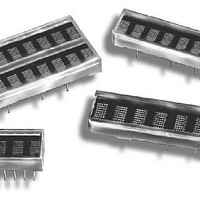
LED DISPLAY 5X7 8CHAR 3.8MM BLUE
Manufacturer
Avago Technologies US Inc.
Series
HCMS-29xxr
Datasheet
1.HCMS-2919.pdf
(14 pages)
Specifications of HCMS-2919
Display Type
Alphanumeric
Millicandela Rating
*
Size / Dimension
1.40" L x 0.40" W x 0.20" H (35.6mm x 10.2mm x 5.1mm)
Color
Blue
Configuration
5 x 7
Voltage - Forward (vf) Typ
*
Package / Case
26-DIP
Number Of Digits/alpha
8
Digit/alpha Size
0.15" (3.8mm)
Number Of Digits
8
Illumination Color
Blue
Wavelength
428 nm
Operating Voltage
5.5 V
Maximum Operating Temperature
+ 85 C
Minimum Operating Temperature
- 40 C
Luminous Intensity
170 ucd
Lead Free Status / RoHS Status
Lead free / RoHS Compliant
Common Pin
-
Lead Free Status / Rohs Status
Details


Pixel Map
In a 4-character display, the 160-bits are arranged as
20 columns by 8 rows. This array can be conceptualized
as four 5x8 dot matrix character locations, but only 7
of the 8 rows have LEDs (see Figure 4 & 5). The bottom
row (row 0) is not used. Thus, latch location 0 is never
displayed. Column 0 controls the left-most column.
Data from Dot Latch locations 0-7 determine whether
or not pixels in Column 0 are turned-on or turned off.
Therefore, the lower left pixel is turned-on when a logic
high is stored in Dot Latch location 3. Characters are
loaded in serially, with the left-most character being
loaded first and the right-most character being loaded
last. By loading one character at a time and latching
the data before loading the next character, the figures
will appear to scroll from right to left.
Control Register
The Control Register allows software modification of
the IC’s operation and consists of two independent 7-
bit control words. Bit D
one of the two 7-bit control words. Control Word 0
performs pulse width modulation brightness control,
peak pixel current brightness control, and sleep mode.
Control Word 1 sets serial/simultaneous data out mode,
and external oscillator prescaler. Each function is
independent of others.
Figure 5. Block diagram
REGISTER
8
DATA IN
SELECT
SELECT
BLANK
ENABLE
RESET
OSC
OSC
CHIP
CLK
L
H
D Q
(LATCHED)
÷8
OSCILLATOR
RS
PRESCALE
H
L
DATA IN
CLR
VALUE
7
H
in the shift register selects
H
L
L
RST
REFRESH
CONTROL
REGISTER
CONTROL
SER/PAR
MODE
PWM BRIGHTNESS
RS (LATCHED)
REFERENCE
CURRENT
DATA
CONTROL
OUT
H
GND (LED)
H
L
Figure 4. Pixel Map
DATA TO
NEXT
CHARACTER
COLUMN 0
L
DO
0
CHAR 0
40 BIT
S.R.
x x x x
DATA OUT
DI
ANODE
DO
x x x x x
CHAR 1
40 BIT
S.R.
PIXEL
DI
CURRENT SOURCES
x x x x x
DO
CHAR 2
40 BIT
S.R.
DI
x x x x x
DO
CHAR 3
40 BIT
S.R.
COLUMN 19
DI
ROW 7
ROW 1
ROW 0 (NO LEDS)
DOT
REGISTER
BIT # 159
DOT
REGISTERS
AND
LATCHES
V LED +
DATA FROM
PREVIOUS
CHARACTER
ROW 0
(NOT USED)
ROW 7
ROW 6
ROW 5
ROW 4
ROW 3
ROW 2
ROW 1
Related parts for HCMS-2919
Image
Part Number
Description
Manufacturer
Datasheet
Request
R

Part Number:
Description:
LED DISPLAY 5X7 4CHAR 5MM GREEN
Manufacturer:
Avago Technologies US Inc.
Datasheet:

Part Number:
Description:
LED DISPLAY 5X7 8CHAR 3.8MM YLW
Manufacturer:
Avago Technologies US Inc.
Datasheet:

Part Number:
Description:
LED DISPLAY 5X7 4CHAR 3.8MM YLW
Manufacturer:
Avago Technologies US Inc.
Datasheet:

Part Number:
Description:
LED DISPLAY 5X7 4CHAR 3.8MM ORN
Manufacturer:
Avago Technologies US Inc.
Datasheet:

Part Number:
Description:
LED DISPL 5X7 4CHAR 3.8MM ALGAAS
Manufacturer:
Avago Technologies US Inc.
Datasheet:
Part Number:
Description:
LED DISPLAY 5X7 4CHAR 3.8MM RED
Manufacturer:
Avago Technologies US Inc.
Datasheet:
Part Number:
Description:
LED DISPLAY 5X7 4CHAR 3.8MM ORN
Manufacturer:
Avago Technologies US Inc.
Datasheet:
Part Number:
Description:
LED DISPLAY 5X7 4CHAR 3.8MM YLW
Manufacturer:
Avago Technologies US Inc.
Datasheet:
Part Number:
Description:
LED DISPLAY 5X7 4CHAR 5MM YLW
Manufacturer:
Avago Technologies US Inc.
Datasheet:
Part Number:
Description:
LED DISPLAY 5X7 4CHAR 5MM ORN
Manufacturer:
Avago Technologies US Inc.
Datasheet:
Part Number:
Description:
LED DISPLAY 5X7 4CHAR 5MM GRN
Manufacturer:
Avago Technologies US Inc.
Datasheet:
Part Number:
Description:
LED DISPLAY 5X7 4CHAR 5MM RED
Manufacturer:
Avago Technologies US Inc.
Datasheet:
Part Number:
Description:
LED DISPLAY 5X7 4CHAR 3.8MM RED
Manufacturer:
Avago Technologies US Inc.
Datasheet:
Part Number:
Description:
LED DISPLAY 5X7 4CHAR 3.8MM GRN
Manufacturer:
Avago Technologies US Inc.
Datasheet:
Part Number:
Description:
LED DISPLAY 5X7 4CHAR 5MM GRN
Manufacturer:
Avago Technologies US Inc.
Datasheet: