M0216SD-162SDAR2-1 Newhaven Display, M0216SD-162SDAR2-1 Datasheet
M0216SD-162SDAR2-1
Specifications of M0216SD-162SDAR2-1


Related parts for M0216SD-162SDAR2-1


M0216SD-162SDAR2-1 Summary of contents
Page 1
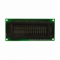
... M0216SD‐162SDAR2-1 Vacuum Fluorescent Display Module RoHS Compliant ...
Page 2
... SCOPE This specification applies to VFD module (Model NO: M0216SD-162SDAR2-1) . 2.0 FEATURES *Since a DC/DC converter is used, only +5Vdc power source is required to operate the module. *5x8 dot matrix display, DC-DC/AC converter, and controller/driver circuitry. *High quality display and luminance. *ASCII and Japanese characters (CG-ROM font). ...
Page 3
... Dot size (mm) Dot pitch (mm) Peak wavelength of illumination 2 Luminance (cd/m / fL) STANDARD NAME width height width height Green (505 nm 0.235 0.405 min. typ. VALUE dot matrix 5.34 2.10 3.30 6.16 0.34 0.58 0.44 0.68 350 / 102 500 / 146 DOCUMENT NO. REV. NO. 03 M0216SD-162SDAR2-1 PAGE 3/24 ...
Page 4
... MECHANICAL DRAWINGS STANDARD S NAME REV. NO. DOCUMENT NO. M0216SD-162SDAR2-1 03 PAGE 4/24 ...
Page 5
... Hstg Symbol Min -0.3 IN DOCUMENT NO. M0216SD-162SDAR2 FLUORESCENT DISPLAY ( Comment Without condensation Without condensation Total amplitude: 1.5mm Freq sine wave Sweep time: 1 min./cycle Duration: 2 hrs./axis (X,Y,Z) Duration: 11ms Waveform: half sine wave 3 times/axis (X,Y,Z,-X,-Y,-Z) Max. Unit 6 +0.3 ...
Page 6
... CC V 0.8*V - IH1 CC V 0.0 - IL1 V 0.7*V - IH2 CC V 0.0 - IL2 -500 - I Symbol Min RVCC t 1 OFF t 100 IRSTD t 100 ERSTD t 500 RSTL the reference points. CC DOCUMENT NO. M0216SD-162SDAR2-1 Max. Unit 5 220 0.2 0.3 0.5 V 1.0 uA Max. Unit REV. NO. PAGE 03 6/24 ...
Page 7
... Note: All timing is specified using 20% and 80 STANDARD NAME t RVCC 4.5V 0.2V t OFF Figure 1. Power-up Internal Reset Timing RSTL Figure 2. External Reset Timing Symbol Min 230 EH PW 230 500 CYCE DHR as the reference points. CC DOCUMENT NO. M0216SD-162SDAR2-1 t IRSTD t ERSTD Max. Unit 160 REV. NO. 03 PAGE 7/24 ...
Page 8
... Figure 3. Motorola M68-Type Parallel Interface Write Cycle Timing Figure 4. Motorola M68-Type Parallel Interface Read Cycle Timing STANDARD NAME CYCE CYCE DHR DOCUMENT NO. REV. NO. M0216SD-162SDAR2-1 03 PAGE 8/24 ...
Page 9
... STANDARD NAME Symbol Min RSS t 10 RSH WRL t 100 WRH t 30 DSi t 10 DHi t 166 CYCWR t 166 CYCRD t 70 RDL t 70 RDH t DDi t DHRi as the reference points RSS WRL t DSi M0216SD-162SDAR2-1 Max. Unit - RSH t WRH t DHi DOCUMENT NO. REV. NO. 03 PAGE 9/24 ...
Page 10
... NAME t RSS RDL t DDi t CYCRD Symbol Min. t 100 STBS t 500 STBH 500 WSTB t 200 SCKH t 200 SCKL t 100 DSs t 100 DHs t 500 CYCSCK t WAIT t DDs t DHRs as the reference points. CC DOCUMENT NO. t RSH t RDH t DHRi Max. Unit - 150 REV. NO. M0216SD-162SDAR2-1 03 PAGE 10/24 ...
Page 11
... STBS Figure 7. Synchronous Serial Interface Write Cycle Timing STBS Figure 8. Synchronous Serial Interface Read Cycle Timing STANDARD NAME SCKH t SCKL DSs SCKH t SCKL t DHRs STBH STBH t r REV. NO. DOCUMENT NO. 03 M0216SD-162SDAR2-1 PAGE 11/24 ...
Page 12
... E when R/W is high IB7 IB3 IB6 IB2 IB5 IB1 IB4 IB0 Figure 9. Typical 4-Bit Parallel Interface Sequence Using M68-Type Mode STANDARD NAME IB7 IB3 BF IB6 IB2 IB6 IB5 IB1 IB5 IB4 IB0 IB4 DOCUMENT NO. M0216SD-162SDAR2-1 IB3 IB2 IB1 IB0 REV. NO. 03 PAGE 12/24 ...
Page 13
... SCK. Each read/write cycle begins on the falling edge of STB and ends on the rising edge valid read/write cycle, the STB must go high at the end of the cycle. STANDARD NAME IB7 BF IB6 IB6 IB0 IB0 DOCUMENT NO. M0216SD-162SDAR2 REV. NO. PAGE 13/24 03 ...
Page 14
... This mode allows the modules to be reset by setting the Reset (RST/) input low. STANDARD NAME Start byte R Start byte Instruction / Data Instruction / Data REV. NO. DOCUMENT NO. M0216SD-162SDAR2 PAGE 14/24 03 ...
Page 15
... CHARACTER FONT TABLES RAM (1) CG RAM ( RAM (3) CG RAM ( RAM ( RAM (6) CG RAM ( RAM (8) CG RAM (1) CG RAM ( RAM (3) CG RAM ( RAM ( RAM (6) CG RAM ( RAM (8) STANDARD NAME REV. NO. DOCUMENT NO. 03 M0216SD-162SDAR2-1 PAGE 15/24 ...
Page 16
... DDRAM addresses are 00H to 27H and 40H to 67H. DDRAM not being used for display characters can be used as general purpose RAM. The tables below show the relationship between the DDRAM address and the character position on the VFD before and after a display shift (with the number of display lines set to 2). STANDARD NAME DOCUMENT NO. REV. NO. M0216SD-162SDAR2-1 03 PAGE 16/24 ...
Page 17
... DISPLAY SHIFT DETAIL Relationship before a display shift (non-shifted Relationship after a display shift to the left Relationship after a display shift to the right STANDARD NAME DOCUMENT NO. REV. NO. M0216SD-162SDAR2-1 03 PAGE 17/24 ...
Page 18
... Cursor/display shift Function set CGRAM address set DDRAM address set Address counter read DDRAM or CGRAM write DDRAM or CGRAM read x = don’t care STANDARD NAME: CGRAM address R/W DB7 DB6 DB5 DB4 DB3 DB2 DB1 DB0 BF DOCUMENT NO. M0216SD-162SDAR2-1 CGRAM data CGRAM ( CGRAM ( CGRAM ( ...
Page 19
... DDRAM write. I The AC increments after each DDRAM or CGRAM access the information on the display shifts to the left by one character position after each DDRAM write The display shift function is disabled The display shift function is enabled. STANDARD NAME I/D S REV. NO. DOCUMENT NO. 03 M0216SD-162SDAR2-1 PAGE 19/24 ...
Page 20
... AC contents (cursor position Decrements by one 0 1 Increments by one 1 0 Decrements by one 1 1 Increments by one STANDARD NAME row of pixels S/C No change No change Shifts one character position to the left Shifts one character position to the right R Information on the display DOCUMENT NO. REV. NO. 03 M0216SD-162SDAR2-1 PAGE 20/24 ...
Page 21
... This instruction places the 7-bit DDRAM address specified by DB6-DB0 into the AC (cursor position). Subsequent data writes (reads) will be to (from) DDRAM. DDRAM and CGRAM contents are not affected by this instruction. STANDARD NAME CGRAM address 0 1 DDRAM address N x BR1 BR0 DOCUMENT NO. REV. NO. M0216SD-162SDAR2-1 PAGE 21/24 03 ...
Page 22
... I/D and S bits set by the Entry Mode Set instruction. Before sending this instruction, a DDRAM or CGRAM Address Set instruction should be executed to set the AC to the desired DDRAM or CGRAM address to be read. STANDARD NAME 1 BF=0 AC contents 0 Write data 1 Read data DOCUMENT NO. REV. NO. M0216SD-162SDAR2-1 03 PAGE 22/24 ...
Page 23
... The modules can be initialized by using instructions if the modules are not reset according to the reset timing detailed in Section 3.7.1 (Reset Timing). After any reset, the function set command must be the first instruction sent to the module. STANDARD NAME Sets the luminance level to 100%. REV. NO. DOCUMENT NO. 03 M0216SD-162SDAR2-1 PAGE 23/24 ...
Page 24
... Parallel data Transfer mode Open Serial data Transfer mode Paralle Parallel Serial (Intel) (Motorola) VCC VCC STB RS SCK RD/ NC DB1 NC DB3 NC DB5 NC DB7 FUNCTION MPU type Selection External Reset Section FUNCTION DOCUMENT NO. REV. NO. 03 M0216SD-162SDAR2-1 VCC RS E DB1 DB3 DB5 DB7 PAGE 24/24 ...