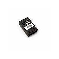
AFBR-5805Z Avago Technologies US Inc., AFBR-5805Z Datasheet - Page 10

AFBR-5805Z
Manufacturer Part Number
AFBR-5805Z
Description
TXRX ATM SONET OC3 3V SC 1X9
Manufacturer
Avago Technologies US Inc.
Series
-r
Specifications of AFBR-5805Z
Wavelength
1310nm
Applications
General Purpose
Voltage - Supply
3.3V
Connector Type
SC
Mounting Type
Through Hole
Function
Provides the system designer with products to implement a range of soluntions for multimode fiber SONET OC-3 (SDH STM-1)
Product
Transceiver
Data Rate
155 Mbps
Maximum Rise Time
3 ns/2.2 ns
Maximum Fall Time
3 ns/2.2 ns
Pulse Width Distortion
1.2 ns (Max)/1.91 ns (Max)
Maximum Output Current
50 mA
Operating Supply Voltage
3.135 V to 3.5 V or 4.75 V to 5.25 V
Maximum Operating Temperature
+ 70 C
Minimum Operating Temperature
0 C
Package / Case
SIP-9
Lead Free Status / RoHS Status
Lead free / RoHS Compliant
For Use With
Multimode Glass
Lead Free Status / RoHS Status
Lead free / RoHS Compliant, Lead free / RoHS Compliant
Available stocks
Company
Part Number
Manufacturer
Quantity
Price
Company:
Part Number:
AFBR-5805Z
Manufacturer:
Avago Technologies
Quantity:
135
Immunity
Equipment utilizing these transceivers will be subject to
radio-frequency electromagnetic fields in some environ-
ments. These transceivers have a high immunity to such
fields.
Transceiver Reliability and Performance Qualification Data
The 1 x 9 transceivers have passed Avago Technologies’
reliability and performance qualification testing and
are undergoing ongoing quality monitoring. Details are
available from your Avago Technologies sales represen-
tative.
Ordering Information
The AFBR-5805Z/-5805TZ 1300 nm products are avail-
able for production orders through the Avago Tech-
nologies Component Field Sales Offices and Authorized
Distributors world wide.
Absolute Maximum Ratings
10
Parameter
Storage Temperature
Lead Soldering Temperature
Lead Soldering Time
Supply Voltage
Data Input Voltage
Differential Input Voltage
Output Current
Stresses in excess of the absolute maximum ratings can cause catastrophic damage to the device. Limits apply to each param-
eter in isolation, all other parameters having values within the recommended operating conditions. It should not be assumed
that limiting values of more than one parameter can be applied to the product at the same time. Exposure to the absolute
maximum ratings for extended periods can adversely affect device reliability.
Symbol
T
T
t
V
V
V
I
O
SOLD
S
SOLD
CC
I
D
Min.
-40
-0.5
-0.5
Figure 10. Relative Input Optical Power vs. Eye Sampling Time
Position.
5
4
3
2
1
0
-3
CONDITIONS:
1. T
2. V
3. INPUT OPTICAL RISE/FALL TIMES = 1.0/2.1 ns.
4. INPUT OPTICAL POWER IS NORMALIZED TO
5. NOTE 16 AND 17 APPLY.
CENTER OF DATA SYMBOL.
A
CC
EYE SAMPLING TIME POSITION (ns)
= +25˚ C
= 3.3 V to 5 V dc
-2
Typ.
AFBR-5805Z SERIES
-1
0
Max.
+100
+260
10
.0
V
1.4
50
CC
1
2
Unit
°C
°C
sec.
V
V
V
mA
3
Reference
Note 1


