HFBR-1119TZ Avago Technologies US Inc., HFBR-1119TZ Datasheet - Page 4
HFBR-1119TZ
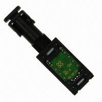
Manufacturer Part Number
HFBR-1119TZ
Description
XMITTER FIBER OPTIC 266MBD ST
Manufacturer
Avago Technologies US Inc.
Datasheet
1.HFBR-2119TZ.pdf
(12 pages)
Specifications of HFBR-1119TZ
Wavelength
1300nm
Spectral Bandwidth
137nm
Voltage - Forward (vf) Typ
7V
Current - Dc Forward (if)
185mA
Connector Type
ST
Function
Fiber Channel applications or for general purpose fiber optic data link transmission
Product
Transmitter
Data Rate
266 MBd
Maximum Rise Time
2 ns
Maximum Fall Time
2.2 ns
Pulse Width Distortion
0.3 ns
Maximum Output Current
50 mA
Operating Supply Voltage
4.5 V to 5.5 V
Maximum Operating Temperature
+ 70 C
Minimum Operating Temperature
0 C
Package / Case
DIP With Connector
Lead Free Status / RoHS Status
Lead free / RoHS Compliant
Capacitance
-
Voltage - Dc Reverse (vr) (max)
-
Lead Free Status / Rohs Status
Lead free / RoHS Compliant
For Use With
Multimode Glass
Lead Free Status / RoHS Status
Lead free / RoHS Compliant, Lead free / RoHS Compliant
Other names
516-2031
Available stocks
Company
Part Number
Manufacturer
Quantity
Price
Company:

Part Number:
HFBR-1119TZ
Manufacturer:
AVAGO
Quantity:
134


Transmitter and Receiver Signaling
Rate Range and BER Performance
For purposes of definition, the
symbol rate (Baud), also called
signaling rate, is the reciprocal of
the symbol time. Data rate (bits/
sec) is the symbol rate divided by
the encoding factor used to encode
the data (symbols/bit).
The specifications in this data
sheet have all been measured using
the standard Fibre Channel symbol
rate of 266 MBd.
The data link modules can be used
for other applications at signaling
rates different than specified in this
data sheet. Depending on the
actual signaling rate, there may be
some differences in optical power
budget. This is primarily caused by
a change in receiver sensitivity.
These data link modules can also
be used for applications which
require different bit-error-ratio
(BER) performance. Figure 5
illustrates the typical trade-off
between link BER and the receiver
input optical power level.
Data Link Jitter Performance
The Avago 1300 nm data link
modules are designed to operate
per the system jitter allocations
stated in FC-PH Annex A.4.3 and
A.4.4.
The 1300 nm transmitter will
tolerate the worst-case input
electrical jitter allowed, without
violating the worst-case output
optical jitter requirements.
The 1300 nm receiver will tolerate
the worst-case input optical jitter
allowed without violating the
worst-case output electrical jitter
allowed.
4
The jitter specifications stated in
the following transmitter and
receiver specification tables are
derived from the values in FC-PH
Annex A.4.3 and A.4.4. They
represent the worst-case jitter
contribution that the transmitter
and receiver are allowed to make
to the overall system jitter without
violating the allowed allocation. In
practice, the typical jitter contribu-
tion of the Avago data link modules
is well below the maximum allowed
amounts.
Recommended Handling Precautions
It is advised that normal static pre-
cautions be taken in the handling
and assembly of these data link
modules to prevent damage which
may be induced by electrostatic
discharge (ESD). The HFBR-
1119TZ/-2119TZ series meets MIL-
STD-883C Method 3015.4 Class 2.
Figure 5. HFBR-1119TZ/2119TZ bit-error-ratio
vs. relative receiver input optical power.
1 x 10
1 x 10
1 x 10
1 x 10
1 x 10
1 x 10
1 x 10
1 x 10
1 x 10
1 x 10
1 x 10
-10
-11
-12
-2
-3
-4
-5
-6
-7
-8
-9
CONDITIONS:
1. 266 MBd
2. PRBS 2
3. T
4. V
5. INPUT OPTICAL RISE/FALL TIMES =
RELATIVE INPUT OPTICAL POWER – dB
-6
1.0/1.9 ns
A
CC
= 25 °C
= 5 Vdc
-4
7
-1
CENTER OF SYMBOL
-2
0
2
Care should be taken to avoid
shorting the receiver Data or
Signal Detect Outputs directly to
ground without proper current-
limiting impedance.
Solder and Wash Process
Compatibility
The transmitter and receiver are
delivered with protective process
caps covering the individual ST*
ports. These process caps protect
the optical subassemblies during
wave solder and aqueous wash
processing and act as dust covers
during shipping.
These data link modules are
compatible with either industry
standard wave- or hand-solder
processes.
Shipping Container
The data link modules are
packaged in a shipping container
designed to protect it from
mechanical and ESD damage
during shipment or storage.
Board Layout–Interface Circuit and
Layout Guidelines
It is important to take care in the
layout of your circuit board to
achieve optimum performance
from these data link modules.
Figure 6 provides a good example
of a power supply filter circuit that
works well with these parts. Also,
suggested signal terminations for
the Data, Data-bar, Signal Detect
and Signal Detect-bar lines are
shown. Use of a multilayer,
ground-plane printed circuit board
will provide good high-frequency
circuit performance with a low
inductance ground return path. See
additional recommendations noted
in the interface schematic shown in
Figure 6.
Related parts for HFBR-1119TZ
Image
Part Number
Description
Manufacturer
Datasheet
Request
R

Part Number:
Description:
FIBER OPTIC CBL SIMPLEX 1=100M
Manufacturer:
Avago Technologies US Inc.
Datasheet:

Part Number:
Description:
FIBER OPTIC CBL SIMPLEX 1=500M
Manufacturer:
Avago Technologies US Inc.
Datasheet:

Part Number:
Description:
FIBER OPTIC CONN LATCH GRY SIMPL
Manufacturer:
Avago Technologies US Inc.
Datasheet:

Part Number:
Description:
FIBER OPTIC CONN LATCH BLU SIMPL
Manufacturer:
Avago Technologies US Inc.
Datasheet:

Part Number:
Description:
XMITTER VERSATILE LINK HORZ
Manufacturer:
Avago Technologies US Inc.
Datasheet:

Part Number:
Description:
Fiber Optic Transmitters, Receivers, Transceivers 1300nm 155MBd 16-pin DIP ST Rx
Manufacturer:
Avago Technologies US Inc.

Part Number:
Description:
FIBER OPTIC CBL DUPLEX 1=100M
Manufacturer:
Avago Technologies US Inc.
Datasheet:
Part Number:
Description:
FIBER OPTIC CBL SIMPLEX 1=500M
Manufacturer:
Avago Technologies US Inc.
Datasheet:
Part Number:
Description:
FIBER OPTIC CBL DUPLEX 1=500M
Manufacturer:
Avago Technologies US Inc.
Datasheet:

Part Number:
Description:
FIBER OPTIC CBL SIMPLEX 1=100M
Manufacturer:
Avago Technologies US Inc.
Datasheet:

Part Number:
Description:
OPTOCOUPLER GATE DRV 2A 16-SOIC
Manufacturer:
Avago Technologies US Inc.
Datasheet:
Part Number:
Description:
OPTOCOUPLER 2CH 2.5A 16-SOIC
Manufacturer:
Avago Technologies US Inc.
Datasheet:

Part Number:
Description:
OPTOCOUPLER GATE DRV 0.4A 16SOIC
Manufacturer:
Avago Technologies US Inc.
Datasheet:

Part Number:
Description:
OPTOCOUPLER 2.0A 250KHZ 8-DIP
Manufacturer:
Avago Technologies US Inc.
Datasheet:

Part Number:
Description:
OPTOCOUPLER 2.0A 250KHZ GW 8-SMD
Manufacturer:
Avago Technologies US Inc.
Datasheet: