591-2504-013F Dialight, 591-2504-013F Datasheet - Page 3
591-2504-013F
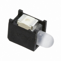
Manufacturer Part Number
591-2504-013F
Description
LED ORANGE PRISM/CBI 606NM SMD
Manufacturer
Dialight
Series
Prism®, CBI®r
Specifications of 591-2504-013F
Color
Orange
Voltage Rating
1.8V
Current
20mA
Lens Style/size
Round, 2.84mm
Configuration
Single
Mounting Type
Surface Mount
Lead Free Status / RoHS Status
Lead free / RoHS Compliant
Lens Type
-
Other names
350-2314-2


Contents
Features............................................................................. 1
Configurations .................................................................. 1
Functional Description..................................................... 1
Logic Block Diagram (CY7C21701KV18)........................ 2
Contents ............................................................................ 3
Pin Configuration ............................................................. 4
Pin Definitions .................................................................. 5
Functional Overview ........................................................ 7
Application Example ........................................................ 8
Truth Table ........................................................................ 9
Write Cycle Descriptions ................................................. 9
IEEE 1149.1 Serial Boundary Scan (JTAG) .................. 10
TAP Controller State Diagram ....................................... 12
Document Number: 001-57344 Rev. *A
165-Ball FBGA (13 x 15 x 1.4 mm) Pinout .................. 4
Read Operations ......................................................... 7
Write Operations ......................................................... 7
Byte Write Operations ................................................. 7
DDR Operation............................................................ 7
Depth Expansion ......................................................... 7
Programmable Impedance .......................................... 7
Echo Clocks ................................................................ 7
Valid Data Indicator (QVLD)........................................ 8
On-Die Termination (ODT) .......................................... 8
PLL .............................................................................. 8
Disabling the JTAG Feature ...................................... 10
Test Access Port—Test Clock................................... 10
Test Mode Select (TMS) ........................................... 10
Test Data-In (TDI) ..................................................... 10
Test Data-Out (TDO)................................................. 10
Performing a TAP Reset ........................................... 10
TAP Registers ........................................................... 10
TAP Instruction Set ................................................... 10
TAP Controller Block Diagram ...................................... 13
TAP Electrical Characteristics ...................................... 13
TAP AC Switching Characteristics ............................... 14
TAP Timing and Test Conditions .................................. 14
Identification Register Definitions ................................ 15
Scan Register Sizes ....................................................... 15
Instruction Codes ........................................................... 15
Boundary Scan Order .................................................... 16
Power Up Sequence in DDR II+ SRAM ......................... 17
Maximum Ratings........................................................... 18
Operating Range............................................................. 18
Neutron Soft Error Immunity ......................................... 18
Electrical Characteristics............................................... 18
Capacitance .................................................................... 20
Thermal Resistance........................................................ 20
Switching Characteristics.............................................. 21
Switching Waveforms .................................................... 22
Ordering Information...................................................... 23
Package Diagram............................................................ 23
Document History Page ................................................. 24
Sales, Solutions, and Legal Information ...................... 24
Power Up Sequence ................................................. 17
PLL Constraints......................................................... 17
DC Electrical Characteristics..................................... 18
AC Electrical Characteristics ..................................... 19
Read/Write/Deselect Sequence ................................ 22
Worldwide Sales and Design Support....................... 24
Products .................................................................... 24
PSoC Solutions ......................................................... 24
CY7C21701KV18
Page 3 of 24
[+] Feedback
Related parts for 591-2504-013F
Image
Part Number
Description
Manufacturer
Datasheet
Request
R

Part Number:
Description:
LED PRISM 3MM RND LC SQ ORN SMD
Manufacturer:
Dialight
Datasheet:
Part Number:
Description:
LED PRISM 3MM RND LC ORN SMD
Manufacturer:
Dialight
Datasheet:
Part Number:
Description:
LED PRISM 3MM RND LC SQ ORN SMD
Manufacturer:
Dialight
Datasheet:
Part Number:
Description:
LED PRISM 3MM RND LC ORN SMD
Manufacturer:
Dialight
Datasheet:
Part Number:
Description:
LED PRISM 3MM RND LC SQ ORN SMD
Manufacturer:
Dialight
Datasheet:

Part Number:
Description:
LED PRISM 3MM GREEN
Manufacturer:
Dialight
Datasheet:

Part Number:
Description:
LED PRISM 3MM RT ANG YELLOW SMT
Manufacturer:
Dialight
Datasheet:

Part Number:
Description:
LED PRISM 3MM RT ANG GREEN SMT
Manufacturer:
Dialight
Datasheet:
Part Number:
Description:
LED PRISM 3MM RA HIEFF RED SMT
Manufacturer:
Dialight
Datasheet:
Part Number:
Description:
LED PRISM 3MM ALGASS RED SMT
Manufacturer:
Dialight
Datasheet:
Part Number:
Description:
LED PRISM 3MM RA ALGAAS RED SMT
Manufacturer:
Dialight
Datasheet:

Part Number:
Description:
LED PRISM 3MM RA SUP RED/GRN SMT
Manufacturer:
Dialight
Datasheet:
Part Number:
Description:
LED PRISM 3MM RT ANG YEL/GRN SMT
Manufacturer:
Dialight
Datasheet:
Part Number:
Description:
LED 3MM PRISM BLUE SMD
Manufacturer:
Dialight
Datasheet:
Part Number:
Description:
LED 3MM PRISM BLUE SMD
Manufacturer:
Dialight
Datasheet: