591-2504-013F Dialight, 591-2504-013F Datasheet - Page 9
591-2504-013F
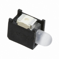
Manufacturer Part Number
591-2504-013F
Description
LED ORANGE PRISM/CBI 606NM SMD
Manufacturer
Dialight
Series
Prism®, CBI®r
Specifications of 591-2504-013F
Color
Orange
Voltage Rating
1.8V
Current
20mA
Lens Style/size
Round, 2.84mm
Configuration
Single
Mounting Type
Surface Mount
Lead Free Status / RoHS Status
Lead free / RoHS Compliant
Lens Type
-
Other names
350-2314-2


Truth Table
The truth table for the CY7C21701KV18 follows.
Write Cycle Descriptions
The write cycle description table for CY7C21701KV18 follows.
Notes
Document Number: 001-57344 Rev. *A
Write Cycle:
Load address; wait one cycle;
input write data on consecutive K and K rising edges.
Read Cycle: (2.5 cycle Latency)
Load address; wait two and half cycles;
read data on consecutive K and K rising edges.
NOP: No Operation
Standby: Clock Stopped
4. X = “Don’t Care,” H = Logic HIGH, L = Logic LOW, ↑ represents rising edge.
5. Device powers up deselected with the outputs in a tri-state condition.
6. “A” represents address location latched by the devices when transaction was initiated. A + 1 represents the address sequence in the burst.
7. “t” represents the cycle at which a read/write operation is started. t + 1 and t + 2 are the first and second clock cycles succeeding the “t” clock cycle.
8. Data inputs are registered at K and K rising edges. Data outputs are also delivered on K and K rising edges.
9. Ensure that when clock is stopped K = K and C = C = HIGH. This is not essential, but permits most rapid restart by overcoming transmission line charging symmetrically.
10. Is based on a write cycle that was initiated in accordance with the
BWS
of a write cycle, as long as the setup and hold requirements are achieved.
H
H
H
H
H
H
H
H
L
L
L
L
0
BWS
H
H
H
H
H
H
H
H
L
L
L
L
1
BWS
H
H
H
H
H
H
H
H
L
L
L
L
Operation
2
BWS
H
H
H
H
H
H
H
H
L
L
L
L
3
L–H
L–H
L–H
L–H
L–H
L–H
K
–
–
–
–
–
–
L–H During the data portion of a write sequence, all four bytes (D
L–H During the data portion of a write sequence, only the lower byte (D
L–H During the data portion of a write sequence, only the byte (D
L–H During the data portion of a write sequence, only the byte (D
L–H During the data portion of a write sequence, only the byte (D
L–H No data is written into the device during this portion of a write operation.
K
–
–
–
–
–
–
[4, 5, 6, 7, 8, 9]
During the data portion of a write sequence, all four bytes (D
the device.
the device.
During the data portion of a write sequence, only the lower byte (D
into the device. D
into the device. D
During the data portion of a write sequence, only the byte (D
the device. D
the device. D
During the data portion of a write sequence, only the byte (D
the device. D
the device. D
During the data portion of a write sequence, only the byte (D
the device. D
the device. D
No data is written into the device during this portion of a write operation.
Write Cycle Descriptions
Stopped
L-H
L-H
L-H
K
[4, 10]
[8:0]
[8:0]
[17:0]
[17:0]
[26:0]
[26:0]
and D
and D
[35:9]
[35:9]
and D
and D
remains unaltered.
remains unaltered.
LD
H
X
L
L
remains unaltered.
remains unaltered.
[35:18]
[35:18]
table. BWS
[35:27]
[35:27]
remains unaltered.
remains unaltered.
remains unaltered.
remains unaltered.
0
R/W
, BWS
H
X
X
L
Comments
1
, BWS
D(A) at K(t + 1) ↑
Q(A) at K(t + 2)↑
High Z
Previous State
2
, and BWS
DQ
CY7C21701KV18
3
can be altered on different portions
[35:0]
[35:0]
[26:18]
[26:18]
[35:27]
[35:27]
[17:9]
[17:9]
D(A+1) at K(t + 1) ↑
Q(A+1) at K(t + 3) ↑
High Z
Previous State
) are written into
) are written into
) is written into
) is written into
) is written into
) is written into
) is written into
) is written into
[8:0]
[8:0]
Page 9 of 24
DQ
) is written
) is written
[+] Feedback
Related parts for 591-2504-013F
Image
Part Number
Description
Manufacturer
Datasheet
Request
R

Part Number:
Description:
LED PRISM 3MM RND LC SQ ORN SMD
Manufacturer:
Dialight
Datasheet:
Part Number:
Description:
LED PRISM 3MM RND LC ORN SMD
Manufacturer:
Dialight
Datasheet:
Part Number:
Description:
LED PRISM 3MM RND LC SQ ORN SMD
Manufacturer:
Dialight
Datasheet:
Part Number:
Description:
LED PRISM 3MM RND LC ORN SMD
Manufacturer:
Dialight
Datasheet:
Part Number:
Description:
LED PRISM 3MM RND LC SQ ORN SMD
Manufacturer:
Dialight
Datasheet:

Part Number:
Description:
LED PRISM 3MM GREEN
Manufacturer:
Dialight
Datasheet:

Part Number:
Description:
LED PRISM 3MM RT ANG YELLOW SMT
Manufacturer:
Dialight
Datasheet:

Part Number:
Description:
LED PRISM 3MM RT ANG GREEN SMT
Manufacturer:
Dialight
Datasheet:
Part Number:
Description:
LED PRISM 3MM RA HIEFF RED SMT
Manufacturer:
Dialight
Datasheet:
Part Number:
Description:
LED PRISM 3MM ALGASS RED SMT
Manufacturer:
Dialight
Datasheet:
Part Number:
Description:
LED PRISM 3MM RA ALGAAS RED SMT
Manufacturer:
Dialight
Datasheet:

Part Number:
Description:
LED PRISM 3MM RA SUP RED/GRN SMT
Manufacturer:
Dialight
Datasheet:
Part Number:
Description:
LED PRISM 3MM RT ANG YEL/GRN SMT
Manufacturer:
Dialight
Datasheet:
Part Number:
Description:
LED 3MM PRISM BLUE SMD
Manufacturer:
Dialight
Datasheet:
Part Number:
Description:
LED 3MM PRISM BLUE SMD
Manufacturer:
Dialight
Datasheet: